
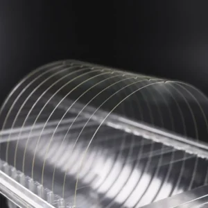
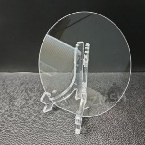
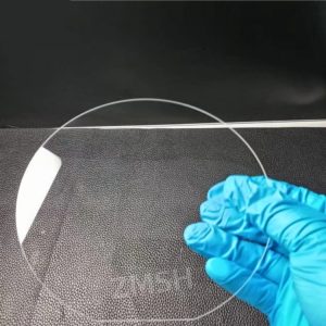
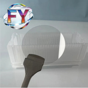
 SiO₂ quartz wafers are ultra-high purity substrates widely used in semiconductor processing, MEMS fabrication, RF devices, and optical systems. Available in standard diameters from 2″ to 12″, these wafers are engineered for applications requiring high thermal stability, optical transparency, and chemical resistance.
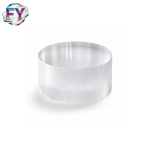
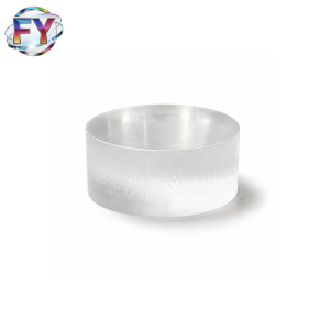
Produced from high-purity fused silica, quartz wafers exhibit a uniform amorphous structure, ensuring consistent performance without internal grain boundaries. Combined with precision polishing and tight thickness control, they provide excellent surface quality for advanced manufacturing processes.
Key Features
- Ultra-high purity (≥99.99% SiO₂) for contamination-sensitive environments
- Wide operating temperature range (stable up to >1100°C)
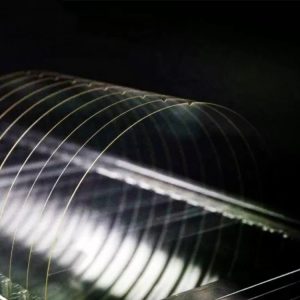
- High optical transmission from UV to near-infrared
- Low thermal expansion coefficient for dimensional stability
- Excellent chemical resistance to acids, alkalis, and solvents
- Ultra-smooth surface finish (Ra ≤ 1 nm) suitable for precision optics and MEMS
Material Characteristics

Quartz wafers are based on amorphous fused SiO₂, offering:
- Isotropic structure with consistent optical behavior
- No birefringence effects common in crystalline materials
- High resistance to thermal shock and plasma exposure
- Low outgassing, suitable for vacuum environments
Compared with conventional glass, quartz wafers provide higher purity, better thermal durability, and broader optical transmission, making them a preferred material in semiconductor and photonics industries.
Specifications
| Spec | Unit | 4″ | 6″ | 8″ | 10″ | 12″ |
|---|---|---|---|---|---|---|
| Diameter / Size | mm | 100 | 150 | 200 | 250 | 300 |
| Tolerance (±) | mm | 0.2 | 0.2 | 0.2 | 0.2 | 0.2 |
| Thickness | mm | ≥0.10 | ≥0.30 | ≥0.40 | ≥0.50 | ≥0.50 |
| Primary Reference Flat | mm | 32.5 | 57.5 | Semi-notch | Semi-notch | Semi-notch |
| LTV (5×5 mm) | μm | <0.5 | <0.5 | <0.5 | <0.5 | <0.5 |
| TTV | μm | <2 | <3 | <3 | <5 | <5 |
| Bow | μm | ±20 | ±30 | ±40 | ±40 | ±40 |
| Warp | μm | ≤30 | ≤40 | ≤50 | ≤50 | ≤50 |
| PLTV (5×5 mm) | % | ≥95 | ≥95 | ≥95 | ≥95 | ≥95 |
| Edge Rounding | mm | SEMI M1.2 / IEC62276 compliant | ||||
| Surface Type | — | SSP / DSP | ||||
| Polished Side Ra | nm | ≤1 | ≤1 | ≤1 | ≤1 | ≤1 |
| Back Side Criteria | μm | 0.2–0.7 or customized |
Applications
Semiconductor Processing
Quartz wafers are widely used as carrier wafers and process components in high-temperature environments such as diffusion, deposition, and etching. Their thermal stability ensures consistent performance during repeated th
ermal cycles.
MEMS & Sensors
In MEMS fabrication, quartz wafers provide stable substrates for microstructures and sensors operatin
g under mechanical and thermal stress conditions.
Optics & Photonics
With excellent UV and IR transmission, quartz wafers are ideal for:
- Optical windows
- Laser components
- Coating substrates
- Precision optical elements
Industrial & Laboratory Use
Quartz wafers are also applied in:
- Plasma chambers and vacuum systems
- Chemical and biomedical analysis
- High-temperature sample carriers
 Manufacturing Process
Quartz wafers are produced through a controlled process to ensure purity and precision:
- Selection of high-purity SiO₂ raw materials
- Melting at approximately 2000°C
- Controlled cooling to form solid quartz blocks
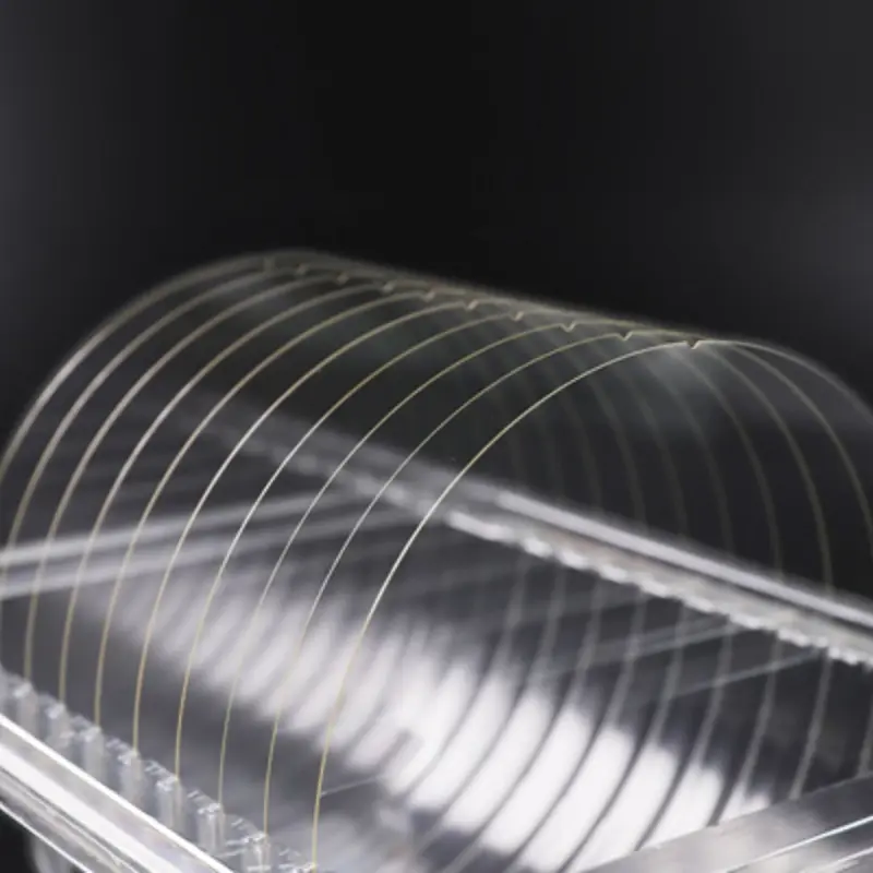
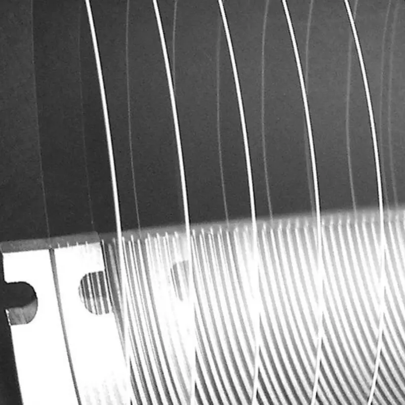
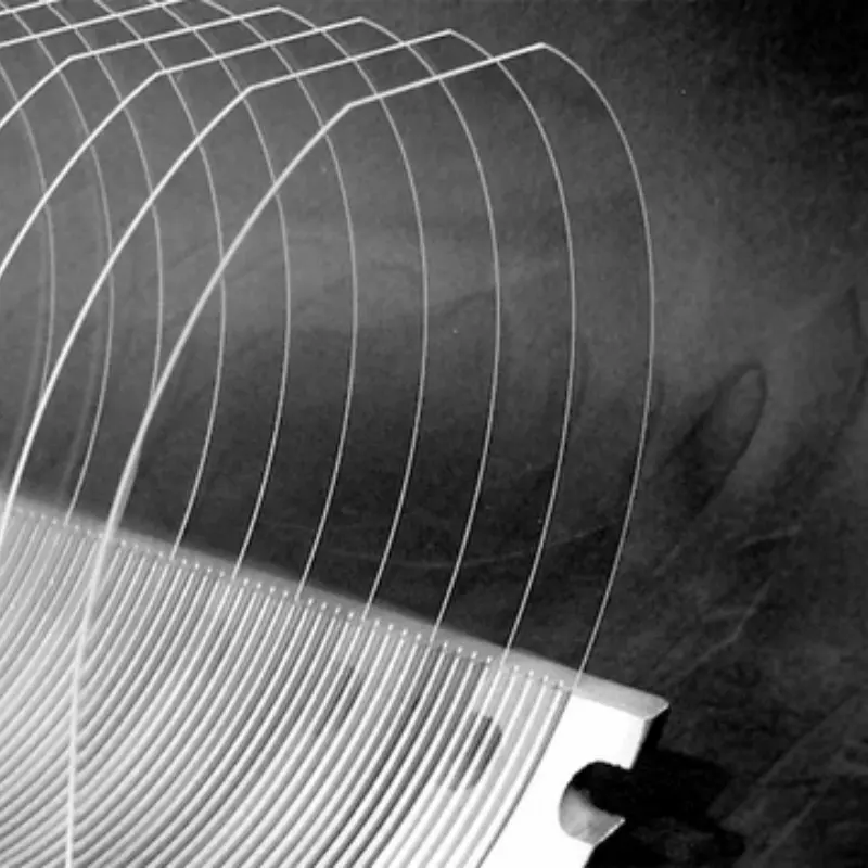
- Precision slicing using wire saws
- Lapping and polishing (single or double side)
- Cleaning and inspection in cleanroom conditions
Customization Options
We provide flexible customization based on application requirements:
- Diameter: 2″–12″ (custom sizes available)
- Thickness: 0.1–6 mm
- Surface finish: SSP / DSP
- Edge type: Notch / Flat / Rounded
- Additional processing:
- Laser drilling
- Patterning
- Optical coatings
FAQ
What is a quartz wafer?
A quartz wafer is a high-purity SiO₂ substrate used in semiconductor, MEMS, and optical applications requiring thermal stability and chemical resistance.
Can quartz wafers withstand high temperatures?
Yes, they can operate continuously at temperatures above 1000°C without deformation.
What makes quartz better than standard glass?
Quartz offers higher purity, superior thermal resistance, and better optical transmission, making it suitable for advanced industrial applications.

Reviews
There are no reviews yet.