
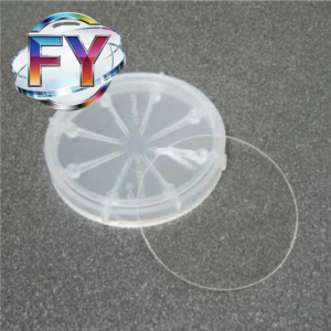
 BOROFLOAT 33 BF33 Glass Wafer for MEMS Wafer Bonding and Optical Packaging
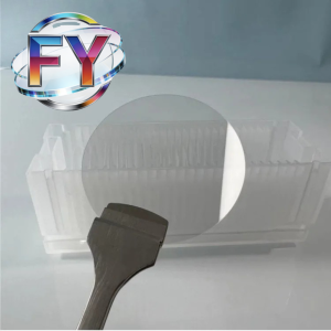
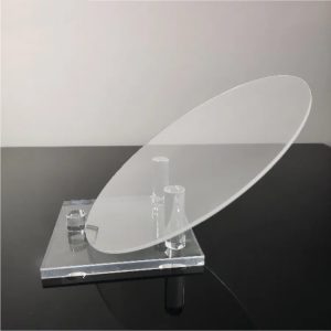
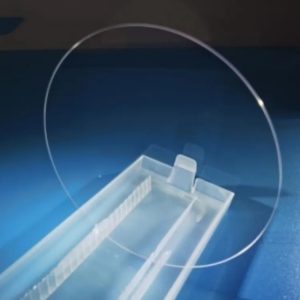
BF33 (BOROFLOAT 33) is a low-expansion borosilicate glass wafer widely used in semiconductor manufacturing, MEMS fabrication, optical packaging, and microfluidic devices. Thanks to its excellent thermal stability, high optical transparency, and superior surface quality, BF33 has become one of the most commonly used glass substrates for silicon bonding applications.
Its coefficient of thermal expansion closely matches silicon, enabling reliable anodic bonding and minimizing thermal stress during high-temperature processing. BF33 wafers are available in various diameters, thicknesses, and polishing grades to meet different wafer-level process requirements.
 주요 이점
주요 이점
- Low thermal expansion coefficient closely matched to silicon
- Excellent anodic bonding compatibility
- High optical transmission from UV to near-infrared wavelengths
- Outstanding chemical resistance against acids and solvents
- High surface flatness and low TTV
- Available in SSP and DSP polishing options
- Suitable for MEMS, microfluidics, and optical packaging
- Stable performance in cleanroom manufacturing environments
기술 사양
| 매개변수 | 가치 |
|---|---|
| 재료 | 붕규산 유리 |
| Grade | BF33 / BOROFLOAT 33 |
| SiO₂ 함량 | >80% |
| 밀도 | 2.23 g/cm³ |
| 굴절률 | 1.47 |
| 열팽창 계수 | 3.3 × 10⁻⁶ /K |
| 스트레인 포인트 | 520°C |
| 어닐링 포인트 | 560°C |
| 연화 포인트 | 820°C |
| Light Transmission | >90% |
| 표면 거칠기 | <1 nm (DSP Available) |
| Water Resistance | ISO Class 1 |
| Acid Resistance | ISO Class 1 |
| Alkali Resistance | ISO Class 2 |
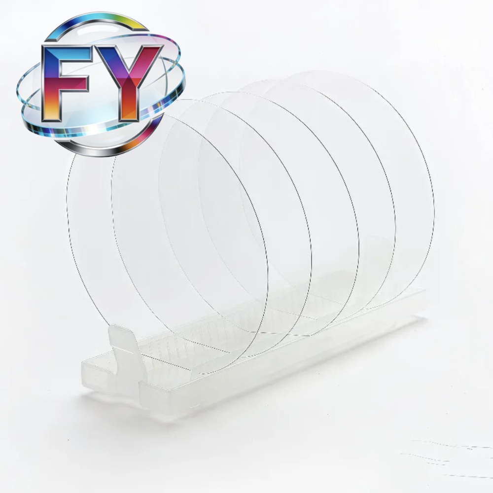
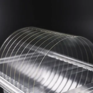
Available Wafer Sizes
| 지름 | 두께 범위 |
| 2 Inch | 100 μm – 2 mm |
| 4 Inch | 100 μm – 3 mm |
| 6 Inch | 200 μm – 5 mm |
| 8 Inch | 300 μm – 5 mm |
| Custom | Available |
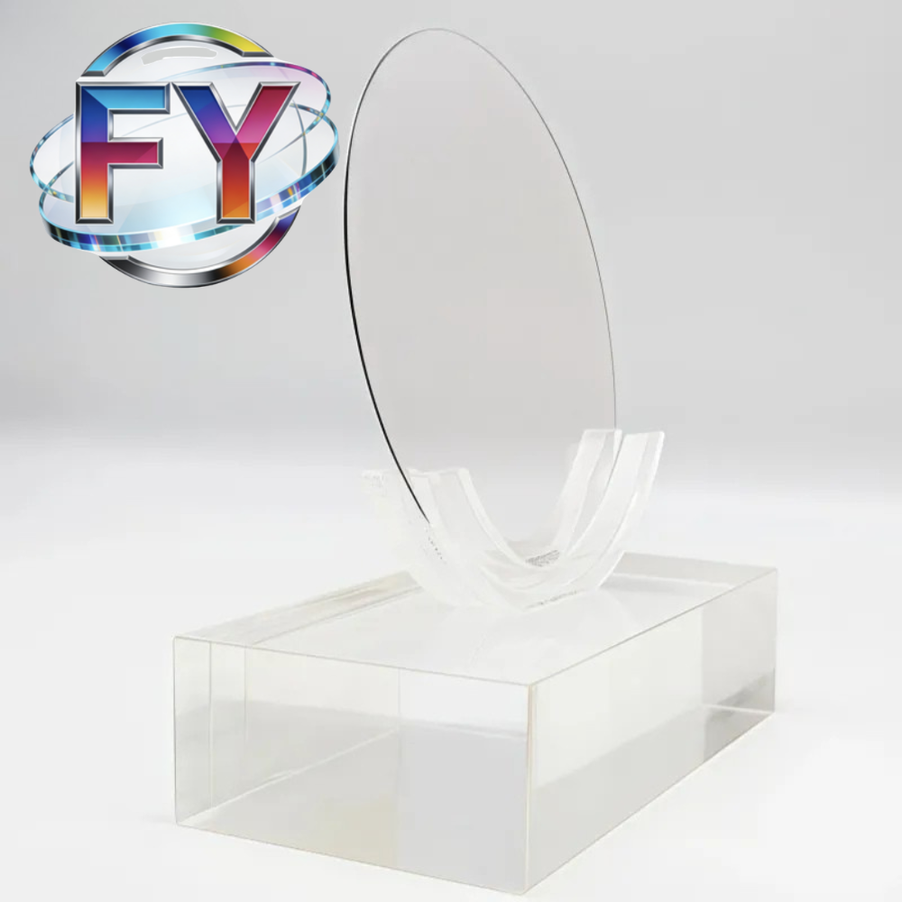
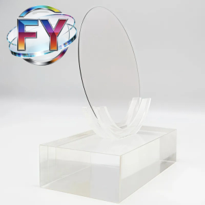
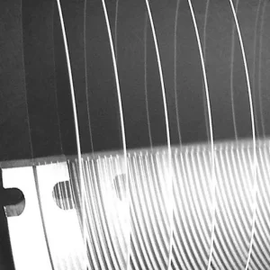
 표면 마감:
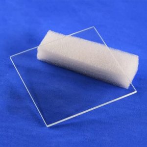
- Single Side Polished (SSP)
- Double Side Polished (DSP)
Edge Type:
- Rounded Edge
- Chamfer Edge
- Custom Machining
일반적인 애플리케이션
MEMS Manufacturing
BF33 glass wafers are widely used as cap wafers and bonding wafers in MEMS sensors, pressure sensors, accelerometers, gyroscopes, and micro-actuators.
Silicon Anodic Bonding
The thermal expansion match between BF33 and silicon makes it an ideal substrate for anodic bonding processes used in wafer-level packaging and hermetic sealing.
미세 유체 장치
BF33 provides excellent transparency and chemical resistance, making it suitable for lab-on-chip devices, microreactors, and biomedical diagnostic systems.
Optical Packaging
The material is commonly used for optical windows, laser packaging, photonic devices, optical filters, and imaging modules.
Semiconductor Process Carriers
BF33 wafers can also serve as carrier wafers for temporary bonding, wafer thinning, and advanced semiconductor packaging processes.
Why Choose BF33 Glass Wafer
Compared with conventional soda-lime glass, BF33 offers significantly better thermal stability, lower thermal expansion, higher optical quality, and superior chemical durability. These advantages make it a preferred substrate material for advanced MEMS fabrication, optical integration, and wafer-level packaging applications.
With excellent flatness, low defect density, and high bonding reliability, BF33 remains one of the most widely adopted glass wafer materials in the semiconductor and photonics industries.
자주 묻는 질문
What is the difference between BF33 and standard glass?
BF33 contains a high percentage of silica and boron oxide, providing lower thermal expansion, better chemical resistance, and higher optical performance than conventional soda-lime glass.
Is BF33 suitable for anodic bonding with silicon?
Yes. BF33 is one of the most commonly used glass materials for silicon anodic bonding because its thermal expansion coefficient closely matches that of silicon.
Can BF33 wafers be supplied with double-side polishing?
Yes. SSP and DSP wafers are available. DSP wafers can achieve surface roughness below 1 nm and are suitable for high-precision wafer bonding applications.
Can custom wafer sizes and thicknesses be provided?
Yes. Custom diameters, thicknesses, edge profiles, and polishing specifications are available according to customer requirements.
상품평
아직 상품평이 없습니다.