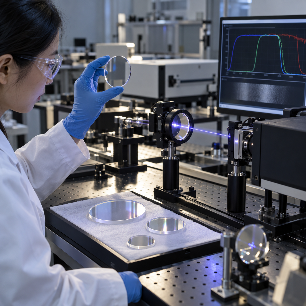
Industry News JGS1 vs JGS2 vs JGS3 Fused Silica: UV–IR Transmission, OH Content, Homogeneity and How to Choose for Optical and Semiconductor Applications Read More »
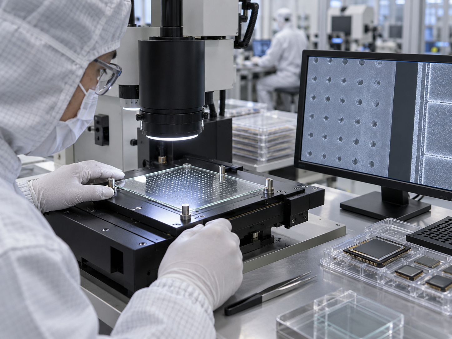
Industry News Semiconductor Glass Substrate Microcracks: Why TGV Drilling, Edge Quality, Warpage and Thermal Stress Matter for AI Packaging Read More »
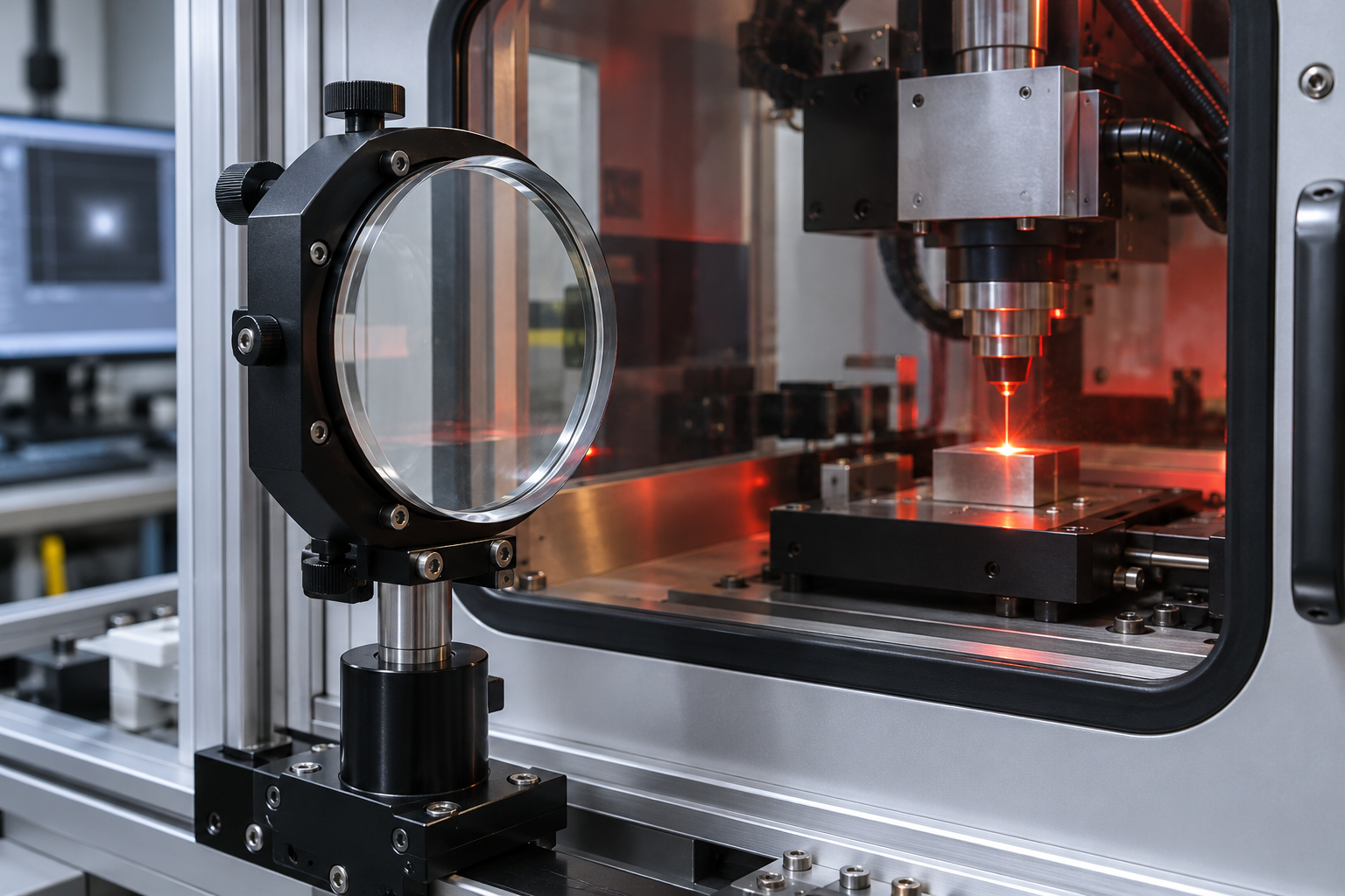
Industry News Fused Silica Optical Components for Laser Material Processing: Wavelength, Surface Quality, Laser Damage Threshold and Custom Fabrication Read More »
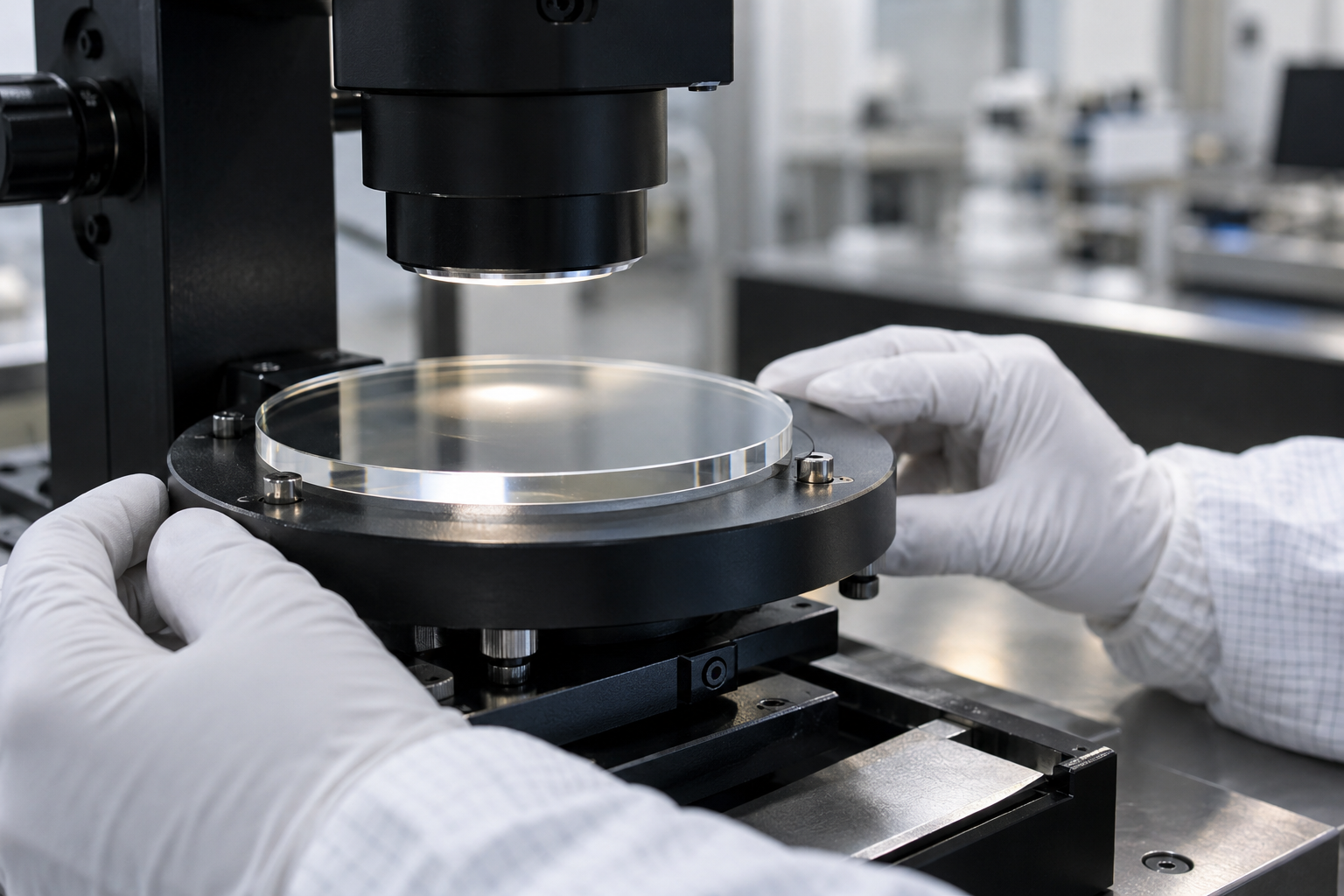
Industry News Quartz Wafer Edge Exclusion: Usable Diameter, Edge Bevel and Inspection Criteria for Custom Orders Read More »
Industry News Custom Quartz Plate Supplier Selection Guide: Purity, Thickness Tolerance, Surface Finish and Inspection Documents Read More »
Industry News ArF-Grade Fused Silica for 193 nm DUV Lithography: Transmission, Homogeneity, Birefringence, Laser Compaction and Coating Requirements Read More »
Industry News Natural Fused Quartz vs Synthetic Fused Silica for Semiconductor Equipment: Purity, OH Content, Trace Metals, Bubble Class and Cost Read More »
Industry News Fused Quartz Carrier Wafers for HBM and Hybrid Bonding: 200mm/300mm Size, TTV, Flatness, Thermal Stability and Laser Debonding Read More »
Industry News Borosilicate Glass Wafers for AI Advanced Packaging: BF33 Properties, CTE, Flatness, TGV Processing and Glass-Core Substrates Read More »
Industry News JGS1 vs JGS2 Fused Silica for UV and Semiconductor Optics: Transmission, OH Content, Laser Damage and Coating Compatibility Read More »