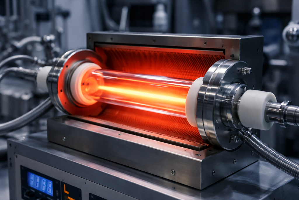
Fused silica is widely used for optical windows, lenses, wafers, laser components and semiconductor equipment because of its high optical transmission, low thermal expansion, chemical stability and resistance to thermal shock.
However, specifications such as JGS1 and JGS2 often create confusion when engineers and purchasing teams select quartz optical components.
Both materials belong to the optical quartz glass family, but they are intended for different wavelength ranges and performance levels. More importantly, the designation “JGS1” or “JGS2” alone is not sufficient for demanding semiconductor or laser applications.
Transmission at the actual operating wavelength, hydroxyl content, optical homogeneity, inclusions, residual stress, surface quality, laser-induced damage resistance and coating requirements should all be considered.
This guide explains how to select between JGS1 and JGS2 for UV optics, semiconductor optical systems and laser-related applications.
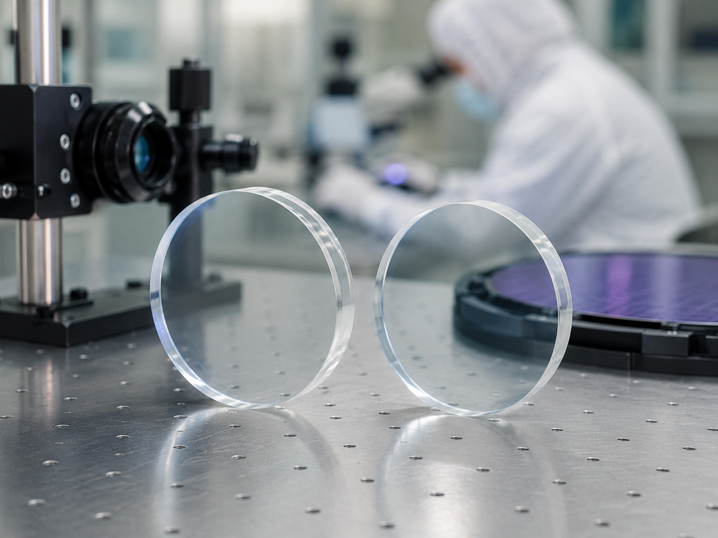
What Are JGS1 and JGS2?
Under the traditional Chinese optical quartz glass classification, JGS materials are divided primarily according to their applicable spectral ranges.
JGS1 is classified as far-ultraviolet optical quartz glass, while JGS2 is classified as ultraviolet optical quartz glass.
The traditional wavelength classifications are approximately:
| Material | Classification | Typical Application Spectral Range |
|---|---|---|
| JGS1 | Far-ultraviolet optical quartz glass | approximately 185–2500 nm |
| JGS2 | Ultraviolet optical quartz glass | approximately 220–2500 nm |
| JGS3 | Infrared optical quartz glass | approximately 260–3500 nm |
This means that JGS1 is normally preferred when transmission below approximately 220 nm is important.
JGS2 is generally suitable when the system operates in the near-UV, visible or near-infrared region and extremely short-wavelength UV transmission is not required.
The JGS classification, however, should not be treated as a complete material specification.
Different manufacturers may use different raw materials, melting processes and impurity-control methods. For precision semiconductor or laser optics, the actual material datasheet should always be reviewed.
JGS1 vs JGS2: Quick Comparison
| Property | JGS1 | JGS2 |
|---|---|---|
| Main optical category | Far-UV fused silica | UV fused quartz/silica |
| Short-wavelength UV performance | Better | More limited |
| Typical lower transmission region | Around 185 nm | Around 220 nm |
| Deep-UV applications | Preferred | Usually not first choice |
| Visible transmission | Excellent | Excellent |
| OH content | Often relatively high depending on manufacturing route | Often lower than synthetic far-UV grades, but supplier dependent |
| Metallic impurity control | Generally better in high-quality synthetic grades | Depends strongly on raw material and process |
| Semiconductor optical use | High-performance UV applications | General UV/visible optical components |
| Laser use | Can be suitable, but laser grade must be specified | Suitable for many general optical systems |
| Cost | Usually higher | Usually more economical |
These differences should be treated as general selection guidance rather than universal guaranteed values.
1. UV Transmission: The Most Important Difference
The first question when choosing between JGS1 and JGS2 should be:
What is the operating wavelength?
For many optical systems, this single parameter immediately narrows the material choice.
JGS1 for Far-UV Transmission
JGS1 is designed for stronger transmission toward the far-ultraviolet region.
It is therefore commonly considered for applications involving wavelengths around:
- 185 nm
- 193 nm
- 200 nm
- Deep-UV spectroscopy
- UV photochemistry
- UV detection systems
For semiconductor applications operating around very short UV wavelengths, synthetic high-purity fused silica is generally more appropriate because metallic impurities and optical defects can cause increased absorption or UV-induced degradation.
However, specifying simply “JGS1” is not sufficient for highly demanding systems such as 193 nm excimer-laser optics.
Additional optical specifications may be required, including:
- Transmission at the exact wavelength
- Internal transmittance
- Optical homogeneity
- Birefringence
- Fluorescence
- Bubble and inclusion grade
- UV solarization resistance
- Laser-induced damage threshold
- Surface roughness
JGS2 for General UV and Visible Optics
JGS2 is widely used when extremely short-wavelength UV transmission is unnecessary.
Typical applications include:
- UV observation windows
- UV curing equipment
- Optical instrument windows
- Semiconductor equipment viewports
- UV lamps
- Inspection systems
- Laboratory optical components
- General precision quartz windows
If the shortest operating wavelength is comfortably above approximately 220 nm, JGS2 may provide sufficient optical performance at a lower material cost.
Therefore, upgrading every quartz optical component to JGS1 does not necessarily improve system performance.
The material should be selected according to wavelength and actual optical requirements.
2. Why OH Content Matters
Hydroxyl groups, normally written as OH, are incorporated into fused silica during certain manufacturing processes.
OH content has an important influence on optical absorption, particularly in infrared wavelength regions.
A well-known hydroxyl-related absorption region occurs around 2.7 µm.
Consequently, high-OH fused silica may provide excellent UV performance while being less suitable for certain infrared applications.
This creates an important material-selection principle:
Lower OH is not automatically better.
For UV optical applications, other properties such as purity, defect concentration and UV stability can be more important than achieving the lowest possible OH concentration.
Conversely, low-OH fused silica becomes especially important when minimizing infrared absorption is the main objective.
Material suppliers therefore offer fused silica grades optimized differently for UV, visible, near-IR and IR applications. Commercial optical-grade fused silica families can vary from below 1 ppm OH to hundreds of ppm depending on their intended wavelength range.
Do Not Specify JGS Grade Based Only on OH
For semiconductor optics, a purchasing specification should not say only:
“JGS1, low OH.”
Instead, specify measurable performance requirements such as:
- Transmission at operating wavelength
- Maximum absorption
- OH limit if necessary
- Metallic impurity limits
- Optical homogeneity
- Bubble/inclusion class
This provides much better control over the final optical performance.
3. JGS1 and JGS2 for Semiconductor Optics
Semiconductor equipment contains many optical components that operate under very different conditions.
Typical fused silica components include:
- UV windows
- Process chamber windows
- Laser entrance windows
- Inspection windows
- Optical wafers
- Beam delivery windows
- Sensor windows
- Alignment optics
- Quartz substrates
- Optical cover plates
The correct material therefore depends on where the quartz component is installed.
Semiconductor Inspection Systems
Wafer and mask inspection systems may use UV illumination to detect increasingly small particles and defects.
Shorter wavelengths can improve optical resolution, but they also place greater demands on fused silica purity and UV transmission.
For these applications, JGS1 or a specified synthetic UV-grade fused silica may be more appropriate than ordinary JGS2.
Semiconductor Process Observation Windows
A chamber viewport used mainly for visible observation does not necessarily require JGS1.
If the optical system operates in visible or near-UV wavelengths, JGS2 may provide sufficient performance while reducing material cost.
The decision should also consider:
- Plasma exposure
- Process gases
- Thermal cycling
- Window thickness
- Coating requirements
- Surface contamination
UV Sensors and Optical Monitoring
UV monitoring equipment used in semiconductor processes may operate at a specific emission or detection wavelength.
Instead of simply selecting the most expensive quartz grade, the designer should compare the transmission curve at that wavelength.
This is particularly important below 250 nm, where material differences become much more significant.
4. Laser Damage: JGS1 Does Not Automatically Mean “Laser Grade”
A common mistake is assuming that any high-transmission JGS1 material will automatically have a high laser-induced damage threshold.
Laser damage is more complicated.
The laser-induced damage threshold, often abbreviated as LIDT, depends on many variables, including:
- Laser wavelength
- Pulse duration
- Repetition rate
- Beam diameter
- Energy density
- Material purity
- Internal defects
- Surface defects
- Subsurface polishing damage
- Surface contamination
- Optical coating
Synthetic fused silica is widely used in high-power laser systems because of its low optical absorption and potentially high laser damage resistance.
But material designation alone cannot guarantee the final LIDT.
Surface Quality Can Be the Limiting Factor
For precision laser optics, damage often initiates at defects close to the optical surface rather than in an ideal region of bulk fused silica.
Possible damage initiation sites include:
- Polishing defects
- Microcracks
- Scratches
- Embedded polishing particles
- Metallic contamination
- Coating defects
Research on UV-irradiated fused silica has shown that substrate preparation and surface microroughness can significantly influence laser damage behavior, including after optical coatings are applied.
Therefore, a laser window specification should include surface-processing requirements instead of relying solely on “JGS1.”
5. Surface Roughness and Subsurface Damage
Surface roughness is particularly important for:
- DUV optics
- High-power laser windows
- Semiconductor inspection systems
- High-precision coated optics
Poor polishing can leave microscopic subsurface cracks even if the optical surface appears clear to the naked eye.
These defects can:
- Increase scattering
- Reduce coating adhesion
- Lower laser damage resistance
- Create contamination sites
- Reduce long-term optical stability
Precision optical fused silica may therefore require surface roughness specified in nanometers or even sub-nanometer ranges depending on the application.
Typical drawings may also specify scratch-dig requirements such as:
- 60/40
- 40/20
- 20/10
- 10/5
The correct specification depends on the optical system rather than the quartz grade alone.
6. Coating Compatibility of JGS1 and JGS2
Both JGS1 and JGS2 can be used as substrates for optical coatings when the material and surface quality are appropriate.
Common coatings include:
- Anti-reflection coatings
- High-reflection coatings
- UV-enhanced coatings
- Dielectric coatings
- Optical filter coatings
- Beam-splitter coatings
Fused silica is particularly attractive as a coating substrate because of its low thermal expansion and good dimensional stability.
However, successful coating performance depends heavily on surface preparation.
Important parameters include:
- Surface roughness
- Surface cleanliness
- Flatness
- Subsurface damage
- Edge quality
- Coating deposition temperature
- Coating stress
UV Coatings Require Extra Attention
Deep-UV coatings are substantially more demanding than ordinary visible-light AR coatings.
At short wavelengths, even small amounts of absorption or contamination can reduce optical performance.
A DUV component should therefore be evaluated as a complete optical system:
fused silica substrate + polished surface + cleaning process + coating stack
rather than evaluating the substrate independently.
For high-power UV systems, coating LIDT must also be considered separately from bulk-material performance.
7. JGS1 for 193 nm: Is It Enough?
This is particularly important for semiconductor applications.
Because traditional JGS1 material can transmit around 193 nm, it may appear suitable for all 193 nm optical systems.
That conclusion is too simple.
ArF excimer lasers operating at 193 nm are used in highly demanding optical applications. Repeated high-energy UV exposure can generate defects in fused silica and change transmission.
For precision 193 nm systems, additional specifications may include:
- Excimer-grade synthetic fused silica
- 193 nm internal transmission
- UV-induced absorption
- Compaction resistance
- Fluorescence
- Optical homogeneity
- Low birefringence
- LIDT
- Inclusion control
Specialized fused silica grades are specifically developed for excimer and UV-damage-resistant applications, demonstrating why wavelength classification alone does not fully define laser performance.
Therefore:
JGS1 can be a starting material category for far-UV applications, but demanding 193 nm semiconductor optics should be specified by actual optical performance rather than JGS1 designation alone.
8. When Should You Choose JGS1?
JGS1 is generally the better starting choice when:
- Operating wavelength extends below approximately 220 nm
- 185 nm transmission is required
- Deep-UV spectroscopy is involved
- High UV purity is important
- UV fluorescence must be minimized
- Semiconductor UV inspection is involved
- Excimer-laser compatibility is required
For demanding laser applications, specify additional laser-grade requirements.
9. When Should You Choose JGS2?
JGS2 may be a more economical choice when:
- Working wavelength is above approximately 220 nm
- Deep-UV transmission is unnecessary
- The component is mainly used in visible light
- The part is an equipment observation window
- Moderate UV transmission is sufficient
- Cost is important
- The component does not experience high-energy laser irradiation
Examples include general UV windows, instrument windows, laboratory optics and many semiconductor equipment viewports.
10. JGS1 vs JGS2 Selection by Application
| Application | Recommended Starting Point |
|---|---|
| 185 nm UV window | JGS1 |
| 193 nm excimer system | Excimer-grade synthetic fused silica / tightly specified JGS1 |
| 248 nm UV optics | JGS1 or qualified UV-grade fused silica |
| 266 nm laser window | Laser-grade fused silica |
| 355 nm laser optics | Laser-grade fused silica |
| General UV equipment window | JGS2 |
| Visible observation window | JGS2 |
| Semiconductor chamber viewport | JGS2 or JGS1 depending on wavelength |
| UV wafer inspection | JGS1 / high-purity synthetic fused silica |
| High-power UV laser | Dedicated laser-grade fused silica |
| IR around 2.7 µm | Low-OH material rather than conventional high-OH JGS1 |
The table should be used only as an initial selection guide. Final material choice must be confirmed according to the actual optical system.
11. What Should Be Specified When Ordering Fused Silica Optics?
For semiconductor and precision optical applications, a complete RFQ should include more than the material name.
Material
Specify:
- JGS1 or JGS2
- Synthetic or natural fused silica if relevant
- Approved manufacturer/grade where required
Optical Wavelength
Specify the actual wavelength or wavelength range.
For example:
- 193 nm
- 248 nm
- 266 nm
- 355 nm
- 400–700 nm
Transmission
Specify minimum required transmission or internal transmission at critical wavelengths.
OH Content
Specify an OH limit only when it is relevant to the optical wavelength or process.
Dimensions
Include:
- Diameter
- Length
- Width
- Thickness
- Dimensional tolerances
Optical Surface
Possible requirements include:
- Surface flatness
- Parallelism
- Wedge
- Surface roughness
- Scratch-dig
- Clear aperture
Edge
Specify:
- Ground edge
- Safety chamfer
- Polished edge
- Bevel dimensions
Coating
Specify:
- AR coating
- HR coating
- Wavelength
- Angle of incidence
- Required reflectance/transmission
- Laser power where relevant
Laser Conditions
For laser optics, provide:
- Wavelength
- CW or pulsed operation
- Pulse duration
- Repetition rate
- Beam diameter
- Maximum energy density
This information is necessary to evaluate whether the substrate, polish and coating are suitable for the application.
Frequently Asked Questions
Is JGS1 better than JGS2?
Not universally.
JGS1 normally offers better far-UV performance, but JGS2 may be perfectly adequate for near-UV and visible optical systems while offering a more economical solution.
The correct material depends primarily on operating wavelength and optical requirements.
What is the main difference between JGS1 and JGS2?
The most practical difference is their short-wavelength UV performance.
JGS1 is traditionally classified for far-UV applications extending toward approximately 185 nm, while JGS2 is generally intended for UV and visible applications beginning around approximately 220 nm.
Does JGS1 always have low OH content?
No.
High-purity synthetic fused silica designed for UV applications can contain significant OH depending on the manufacturing process.
OH content should therefore be confirmed from the actual material certificate rather than assumed from the JGS designation.
Which material is better for semiconductor equipment?
It depends on the component.
JGS2 may be sufficient for a visible observation viewport, while semiconductor UV inspection or DUV optical components may require JGS1 or a dedicated high-purity synthetic fused silica grade.
Which is better for high-power lasers?
Neither JGS1 nor JGS2 alone defines laser performance.
For high-power lasers, specify laser-grade fused silica together with the wavelength, pulse conditions, surface finish and required laser-induced damage threshold.
Can JGS1 and JGS2 be AR coated?
Yes.
Both materials can accept optical coatings when the substrate is properly polished and cleaned. The coating design should match the operating wavelength, angle of incidence, laser power and environmental conditions.
Conclusion
The difference between JGS1 and JGS2 is more than simply one quartz glass being “higher grade” than another.
JGS1 is primarily associated with far-ultraviolet optical performance, while JGS2 is widely used for general UV, visible and semiconductor equipment optical components where extreme short-wavelength transmission is unnecessary.
For advanced semiconductor and laser applications, however, the JGS designation should only be considered the beginning of material selection.
Engineers should also evaluate:
- Transmission at the operating wavelength
- OH content
- Metallic impurities
- Optical homogeneity
- Surface quality
- Subsurface damage
- Laser-induced damage resistance
- Coating performance
- Cleanliness
Selecting the correct fused silica based on actual operating conditions can improve optical performance while avoiding unnecessary material cost.
For custom JGS1 or JGS2 fused silica windows, wafers, plates and precision optical components, drawings should clearly identify wavelength, surface quality, flatness, dimensional tolerance and coating requirements before manufacturing.