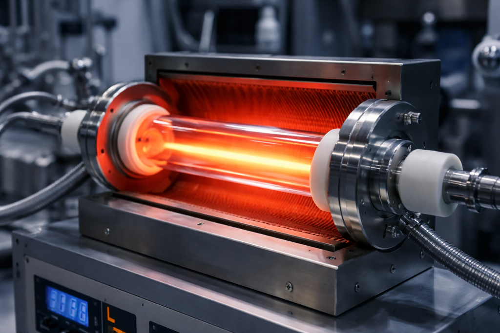
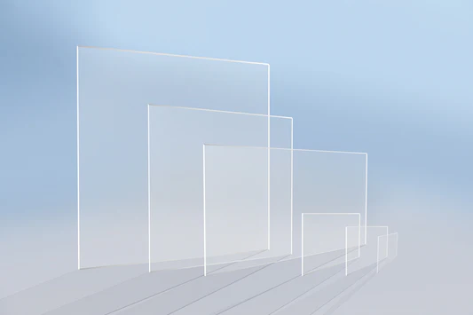
Artificial intelligence is changing not only semiconductor chip architecture but also the materials used to package increasingly large and complex devices.
AI accelerators combine large logic dies, chiplets, high-bandwidth memory (HBM), power-delivery structures and increasingly dense interconnects within a single package. As package dimensions increase, conventional organic substrates face greater challenges in warpage, dimensional stability and fine-line interconnection.
This has accelerated interest in glass substrates, glass interposers and glass-core package substrates.
Among the materials frequently considered for glass wafer processing is borosilicate glass, including BF33-type borosilicate glass.
Its relatively low coefficient of thermal expansion, good flatness, electrical insulation, chemical stability and compatibility with semiconductor processing make it attractive for applications such as:
- Through-glass via substrates
- Glass interposers
- Semiconductor carrier wafers
- Wafer-level packaging
- MEMS substrates
- RF packaging
- Optical packaging
- Advanced package development
However, selecting a borosilicate glass wafer for advanced packaging requires much more than specifying “BF33.”
CTE, wafer thickness, TTV, bow, warp, surface roughness, edge quality, TGV geometry and metallization compatibility all influence process performance.
This guide explains the key considerations.
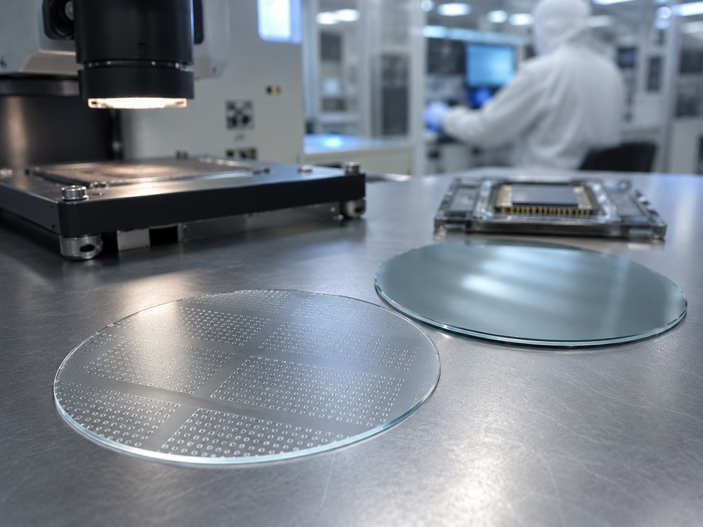
Why Glass Is Receiving More Attention in AI Advanced Packaging
Advanced AI packages are becoming physically larger.
They may integrate:
- GPU or accelerator dies
- Multiple HBM stacks
- Chiplets
- Silicon bridges
- Optical interfaces
- Power-delivery structures
- High-density redistribution layers
As package size increases, controlling substrate deformation becomes more difficult.
Organic package substrates can exhibit significant thermal expansion and warpage during processes such as:
- Lithography
- Die bonding
- Underfill curing
- Reflow
- RDL fabrication
- Thermal cycling
Glass offers several attractive properties for this environment.
These include:
- High dimensional stability
- Low coefficient of thermal expansion
- Excellent surface flatness
- Electrical insulation
- High electrical resistivity
- Potential for fine through-glass vias
- Compatibility with wafer and panel processing
- Possibility of large-format manufacturing
Recent industry investment reflects this interest. Samsung Electro-Mechanics has described glass core as a next-generation package substrate material with lower thermal expansion and better flatness than conventional organic substrates, particularly for large, high-density packages targeting AI and HPC applications.
At the same time, glass substrates remain a developing technology rather than a universal replacement for organic substrates.
TGV formation, metallization, microcrack control, large-panel flatness and thermal-stress management remain major manufacturing challenges.
What Is BF33 Borosilicate Glass?
“BF33” is commonly used in the market to refer to borosilicate 3.3-type flat glass, particularly material comparable to BOROFLOAT® 33.
For precision engineering, however, buyers should not assume that every material sold as “BF33” has exactly the same composition or certified properties.
The actual manufacturer, material grade and datasheet should always be confirmed.
Typical BOROFLOAT® 33 properties include:
| Property | Typical Reference Value |
|---|---|
| Coefficient of thermal expansion, 20–300°C | approximately 3.25 × 10⁻⁶/K |
| Glass transition temperature Tg | approximately 525°C |
| Thermal conductivity at 90°C | approximately 1.2 W/m·K |
| Density | approximately 2.23 g/cm³ |
| Young’s modulus | approximately 64 GPa |
| Poisson’s ratio | approximately 0.20 |
| Dielectric constant at 1 MHz, 25°C | approximately 4.6 |
These are representative material values rather than guaranteed finished-wafer specifications.
For semiconductor packaging, the finished wafer specifications often matter more than the bulk material values.
1. CTE: Why Thermal Expansion Matters
One of the major advantages of borosilicate glass is its relatively low coefficient of thermal expansion.
BOROFLOAT 33 has a reference CTE of approximately:
3.25 × 10⁻⁶/K from 20°C to 300°C.
This is substantially lower than common soda-lime glass and many organic package substrate materials.
Why Low CTE Helps Advanced Packaging
During semiconductor processing, different materials expand and contract at different rates.
A package may contain:
- Silicon
- Copper
- Glass
- Organic dielectric layers
- Mold compound
- Solder
- Adhesives
If their thermal expansion differs significantly, heating can generate mechanical stress.
This may contribute to:
- Wafer bow
- Panel warpage
- Via stress
- Copper delamination
- RDL cracking
- Die misalignment
- Bonding defects
Because borosilicate glass has a CTE relatively close to silicon compared with many polymer-based substrates, it can help reduce dimensional movement during temperature changes.
However, glass does not eliminate CTE mismatch.
Copper, dielectric films and other packaging materials still expand differently.
Therefore, package-level thermal-mechanical simulation remains necessary.
2. Why Flatness Is Important for AI Packaging
Glass is frequently described as having excellent flatness.
This is one of its strongest advantages for advanced packaging.
High flatness helps processes such as:
- Photolithography
- Direct imaging
- Wafer bonding
- Temporary bonding
- Fine-line RDL
- Die placement
- Metrology
- Automated handling
For high-density packaging, even small out-of-plane deformation can affect lithographic focus or alignment.
Raw Glass Flatness vs Finished Wafer Flatness
This distinction is extremely important.
A glass material may have inherently good flatness, but this does not automatically guarantee a semiconductor-grade wafer with low TTV or warp.
Finished wafer geometry depends on:
- Raw glass quality
- Wafer diameter
- Thickness
- Cutting
- Grinding
- Lapping
- Polishing
- Edge processing
- Thermal history
- TGV fabrication
- Metallization
- Film stress
Therefore, a purchase specification should define measurable wafer parameters rather than simply state:
“High-flatness BF33.”
3. TTV, Bow and Warp
For advanced packaging, three geometry specifications are particularly important.
Total Thickness Variation — TTV
TTV represents the difference between the maximum and minimum wafer thickness.
Low TTV is important for:
- Lithography
- Bonding
- Grinding
- CMP
- Uniform copper processing
- Wafer handling
A wafer with poor TTV may create local height differences even if the bulk glass material is highly uniform.
Bow
Bow describes the curvature of the wafer relative to a reference plane.
It is often influenced by:
- Residual mechanical stress
- Film stress
- Thermal processing
- Metallization
- Asymmetric layer stacks
Warp
Warp describes more complex out-of-plane wafer deformation.
For large advanced-packaging substrates, warp becomes increasingly important because larger dimensions amplify alignment and handling problems.
Recent glass-core development highlights this challenge: although glass itself offers excellent dimensional stability, maintaining very high flatness across increasingly large substrates becomes significantly more difficult after vias, copper and multiple build-up layers are added.
4. Why TGV Is Central to Glass Substrates
The key technology enabling glass to function as an electrical packaging substrate is the Through-Glass Via, or TGV.
A TGV is a small hole extending partially or completely through a glass substrate.
After metallization, it provides vertical electrical connection from one side of the substrate to the other.
This is conceptually similar to a through-silicon via, or TSV, but the substrate material is glass.
TGV technology enables glass to serve in:
- Interposers
- RF modules
- Fan-out packaging
- Glass-core substrates
- Sensor packaging
- Optical-electrical integration
- Chiplet integration
Precision glass with through vias has been investigated for semiconductor packaging for many years.
5. How TGVs Are Manufactured
Several methods can be used to form vias in borosilicate glass.
The exact process depends on:
- Glass composition
- Wafer thickness
- Hole diameter
- Pitch
- Aspect ratio
- Production volume
- Required sidewall quality
Common approaches include combinations of:
Ultrafast Laser Processing
Picosecond or femtosecond lasers can locally modify or remove glass.
Advantages may include:
- Small feature size
- Flexible patterns
- Digital processing
- High positioning accuracy
However, inappropriate laser parameters may create:
- Heat-affected regions
- Microcracks
- Taper
- Debris
- Recast material
- Surface damage
Laser-Assisted Chemical Etching
The glass is first modified by laser irradiation and then selectively removed using chemical etching.
This can create higher-aspect-ratio structures with improved sidewall quality.
Direct Laser Drilling
Laser ablation can form vias directly.
The process is comparatively straightforward but via taper and microcrack control may become more challenging as dimensions shrink.
Chemical Processing
Depending on the glass composition and process design, chemical etching may also be combined with masking or other structuring methods.
The correct technique must be matched to the required TGV geometry.
6. TGV Diameter and Aspect Ratio
TGV performance is strongly affected by geometry.
Important parameters include:
- Top diameter
- Bottom diameter
- Via depth
- Wafer thickness
- Sidewall angle
- Pitch
- Aspect ratio
- Sidewall roughness
Smaller vias allow greater interconnect density.
But shrinking the via diameter makes fabrication and metallization much more difficult.
Current industry development shows that TGV remains one of the central technical bottlenecks for glass-core substrates, particularly as via dimensions move toward the sub-10 μm range. Challenges include drilling consistency, microcrack formation and uniform metal deposition inside narrow vias.
7. Microcracks: One of the Main TGV Risks
Glass is strong under appropriate conditions but remains a brittle material.
TGV processing can create microscopic cracks around the via entrance or sidewall.
These cracks may not immediately break the wafer.
However, they can grow during:
- Copper plating
- Thermal cycling
- Bonding
- Mechanical handling
- Assembly
- Reliability testing
Microcrack control therefore becomes essential.
Important variables include:
- Laser energy
- Pulse duration
- Focus position
- Via spacing
- Glass thickness
- Edge distance
- Etching conditions
- Post-process cleaning
Recent glass-substrate development has focused heavily on reducing internal cracking and delamination as the number of build-up layers increases.
8. TGV Metallization
A hole through the glass is only the beginning.
For electrical interconnection, the via must be metallized.
A simplified process may include:
- TGV formation
- Cleaning
- Surface activation
- Seed layer deposition
- Copper plating
- Via filling or conformal metallization
- Surface planarization
- Redistribution layer fabrication
Possible metallization methods may involve:
- PVD
- Sputtering
- Electroless deposition
- Electroplating
The metallization process becomes increasingly difficult as vias become smaller and deeper.
Important requirements include:
- Continuous seed coverage
- Strong adhesion
- Low electrical resistance
- Minimal voids
- Uniform copper deposition
- Controlled thermal stress
High-aspect-ratio vias are particularly challenging because deposition processes must reach deep inside the hole.
9. Why Glass–Copper CTE Mismatch Matters
Glass may provide favorable CTE characteristics compared with organic substrates, but copper expands much more strongly than borosilicate glass.
As the package repeatedly heats and cools, copper-filled TGVs can generate stress at the glass-metal interface.
This can lead to:
- Interfacial delamination
- Glass cracking
- Via deformation
- Reliability degradation
Via diameter, copper thickness, glass thickness and thermal-cycle conditions all influence this behavior.
For high-density TGV designs, mechanical simulation should therefore be considered early in development.
10. Surface Roughness for RDL Processing
Advanced packaging does not require only flat glass.
The surface must also be sufficiently smooth for subsequent thin-film processes.
A rough surface can negatively affect:
- Thin-film uniformity
- Photolithography
- Fine copper lines
- Adhesion
- Bonding
- Electrical performance
Depending on the application, glass wafers may require precision polishing.
Surface roughness can be specified using Ra or RMS values.
For demanding semiconductor processes, nanometer-level surface quality may be required.
However, specifying an unnecessarily low Ra can increase cost significantly.
The correct target should be based on the downstream process.
11. Edge Quality Is Often Overlooked
Glass wafer edges can become failure initiation points.
Poor edge quality may cause:
- Chipping
- Microcracks
- Handling breakage
- Particle contamination
- Reduced thermal-cycle reliability
Typical edge treatments include:
- Ground edges
- Chamfers
- Bevels
- Rounded edges
- Edge polishing
For wafers that will undergo TGV processing and multiple thermal cycles, edge quality should be defined as part of the incoming wafer specification.
12. BF33 as a Carrier Wafer vs a Glass-Core Substrate
This distinction is important for buyers.
BF33 Carrier Wafer
Borosilicate glass is widely suitable as a carrier or support substrate.
Possible applications include:
- Temporary wafer bonding
- Thin-wafer handling
- Wafer thinning
- MEMS processing
- Fan-out packaging
- Bonding development
In this role, important properties include:
- Flatness
- TTV
- Thermal stability
- Surface quality
- Bonding compatibility
BF33 TGV Wafer
A TGV wafer requires additional processing.
Key specifications include:
- Hole diameter
- Pitch
- Aspect ratio
- Taper
- Via position tolerance
- Crack control
- Sidewall quality
Glass-Core Package Substrate
A true glass-core packaging substrate is substantially more complex.
It may contain:
- TGVs
- Copper-filled vias
- Redistribution layers
- Build-up dielectric layers
- Fine copper traces
- Microvias
- Multiple routing layers
Therefore:
BF33 glass wafer ≠ finished glass-core substrate.
The glass wafer is the starting material platform.
13. Why AI Chips Are Driving Glass-Core Development
AI processors are pushing package dimensions and routing density to unprecedented levels.
A modern AI package may require communication among:
- Multiple logic chiplets
- HBM stacks
- I/O dies
- Optical engines
- Power components
This increases the need for:
- Larger package area
- Higher interconnect density
- Better dimensional stability
- Reduced warpage
- Fine-pitch routing
- Better high-frequency performance
This is why glass substrates have become an important advanced-packaging development direction.
In June 2026, TrendForce described AI semiconductor demand as a major driver behind panel-level and glass-core packaging development, while noting that large-area flatness, TGV processing and CTE management remain key barriers to high-volume manufacturing.
In August 2026, industry reporting continued to show increasing development of multilayer glass-core substrates and TGV technologies for AI packaging.
This suggests that glass substrates are moving from research concepts toward increasingly serious industrial validation, although widespread high-volume adoption will still depend on solving process cost and yield challenges.
14. Electrical Properties of BF33
Glass is an electrical insulator.
This can be advantageous compared with conductive silicon interposers in certain applications.
BOROFLOAT 33 has a reference dielectric constant of approximately:
4.6 at 1 MHz and 25°C.
At GHz frequencies, published reference data are around 4.4, although dielectric loss increases with frequency.
These characteristics make borosilicate glass potentially interesting for:
- RF devices
- High-frequency interposers
- Antenna packaging
- Optical interconnect packaging
However, RF packaging designers must evaluate dielectric constant and loss at the actual operating frequency rather than relying on low-frequency datasheet values.
15. BF33 vs Fused Silica for Advanced Packaging
Both borosilicate glass and fused silica can be processed into precision wafers.
They offer different performance and cost characteristics.
| Property | BF33-Type Borosilicate | Fused Silica |
|---|---|---|
| CTE | Low | Extremely low |
| Material cost | Lower | Higher |
| Thermal stability | Good | Excellent |
| Optical UV performance | Moderate | Excellent |
| Semiconductor processing | Good | Excellent |
| TGV processing | Suitable | Suitable but process differs |
| Large-format cost efficiency | Generally favorable | More expensive |
| Carrier wafer use | Excellent | Excellent |
| High-temperature applications | Good | Better |
Fused silica is not automatically the better material.
For many packaging applications, borosilicate glass offers a more practical balance between:
CTE + flatness + machinability + electrical insulation + cost.
16. Typical Glass Wafer Specifications for an RFQ
When requesting borosilicate wafers for semiconductor development, buyers should specify the actual geometry rather than only material type.
Material
- BF33-type borosilicate glass
- Exact manufacturer if required
- Certificate requirement
Wafer Diameter
Common development formats may include:
- 100 mm
- 150 mm
- 200 mm
- 300 mm
Custom rectangular panels may also be used.
Thickness
Possible values may range from thin carrier wafers to several hundred micrometers or more.
Specify:
Thickness ± tolerance
rather than only nominal thickness.
Geometry
Specify:
- TTV
- Bow
- Warp
- Flatness
- Parallelism
Surface
Specify:
- SSP or DSP
- Surface roughness
- Scratch/dig if optical quality is needed
Edge
Specify:
- Chamfer
- Bevel
- Edge polish
- Notch or flat
TGV Requirements
If vias are required, specify:
- Via diameter
- Pitch
- Depth
- Aspect ratio
- Hole taper
- Position tolerance
- Quantity of vias
- Metallized or non-metallized
17. Questions to Ask Before Ordering BF33 Glass Wafers
Before manufacturing, the supplier should understand:
- What is the wafer used for?
- Is it a temporary carrier, interposer or TGV substrate?
- What wafer diameter or panel size is required?
- What thickness is required?
- What are the TTV, bow and warp limits?
- Is one-side or double-side polishing required?
- What surface roughness is required?
- Will TGVs be fabricated?
- What are the TGV diameter and pitch?
- Will the vias be metallized?
- Will the wafer undergo bonding?
- What maximum process temperature will be used?
- Is semiconductor-grade cleaning required?
- What packaging method is required?
Providing this information early can reduce unnecessary machining cost and shorten development cycles.
Frequently Asked Questions
Is BF33 suitable for semiconductor wafers?
Yes.
BF33-type borosilicate glass can be processed into precision glass wafers for semiconductor, MEMS, carrier-wafer and packaging applications.
The finished wafer must still meet application-specific requirements for TTV, flatness, surface finish and cleanliness.
Can BF33 glass be used for TGV processing?
Yes.
Borosilicate glass can be structured using suitable laser and etching processes to create through-glass vias.
The optimum process depends on glass thickness, via diameter, pitch and aspect ratio.
Is BF33 the same as a glass-core substrate?
No.
BF33 is a glass material or wafer substrate.
A finished glass-core package substrate may additionally contain TGVs, copper metallization, RDL and multiple build-up layers.
Why is low CTE important for AI packaging?
AI packages are becoming larger and contain many different materials.
Lower substrate CTE and high dimensional stability can help reduce thermally induced movement and warpage during fabrication and operation.
What is the CTE of BOROFLOAT 33?
SCHOTT publishes a reference coefficient of linear thermal expansion of approximately 3.25 × 10⁻⁶/K between 20°C and 300°C.
What is the most important specification for a glass wafer?
There is no single most important parameter.
For advanced packaging, the combination of:
TTV + bow + warp + surface roughness + thickness + edge quality
usually determines whether the wafer is suitable for downstream processing.
Does lower TTV automatically mean lower warp?
No.
TTV measures thickness uniformity, while warp describes wafer shape.
A wafer can have excellent TTV but still become warped due to residual stress or deposited films.
Can glass replace silicon interposers?
Glass can replace or complement silicon in some interposer architectures, but the technologies have different strengths.
Silicon provides mature fine-feature semiconductor processing, while glass offers electrical insulation, potentially favorable high-frequency properties, large-format capability and strong dimensional stability.
The optimum material depends on the package architecture.
Conclusion
Borosilicate glass wafers are becoming increasingly important as the semiconductor industry explores new materials for AI and high-performance advanced packaging.
BF33-type borosilicate glass offers a useful combination of:
- Low thermal expansion
- Good dimensional stability
- High flatness
- Electrical insulation
- Chemical resistance
- Semiconductor process compatibility
- TGV capability
- Competitive material cost
But material selection alone does not determine packaging success.
For advanced applications, engineers must carefully control:
- Wafer thickness
- TTV
- Bow
- Warp
- Surface roughness
- Edge quality
- TGV diameter and pitch
- Microcracks
- Metallization
- CTE mismatch
The transition from a simple glass wafer to a functional glass-core substrate requires several highly controlled manufacturing steps.
As AI packages continue to increase in size and interconnect density, glass is likely to play a growing role in carrier wafers, TGV interposers and next-generation package substrates.
For custom borosilicate glass wafers, BF33 wafers and TGV glass substrates, the most effective approach is to specify the actual application, dimensions, flatness requirements, surface condition and via geometry before manufacturing begins.