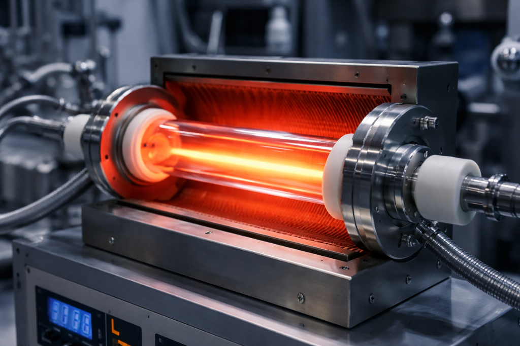
The rapid growth of high-bandwidth memory, chiplets and three-dimensional semiconductor integration is making thin-wafer handling increasingly important. During HBM and hybrid bonding processes, device wafers may undergo temporary bonding, back grinding, TSV reveal, dielectric deposition, redistribution layer processing, polishing and cleaning before the final stacking step.
Once a silicon wafer becomes very thin, it can no longer move through conventional equipment without additional mechanical support. Excessive bow, local stress or handling vibration may cause wafer cracking, edge damage, lithography focus errors or bonding misalignment.
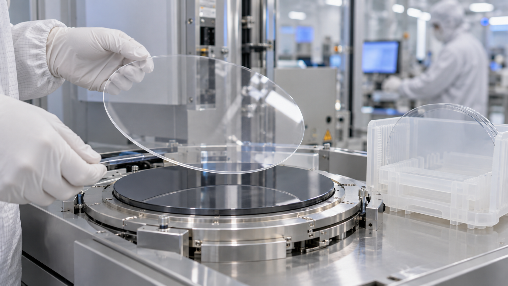
Fused quartz carrier wafers provide a rigid, thermally stable and optically transparent platform for supporting these thin device wafers. Their transparency is particularly valuable in processes that use optical inspection, UV curing or laser-assisted debonding.
However, selecting a quartz carrier involves much more than specifying its diameter. TTV, surface flatness, edge geometry, thermal expansion, optical transmission and compatibility with the temporary bonding material can all affect yield.
Why Carrier Wafers Are Needed in HBM Manufacturing
HBM packages achieve high bandwidth by vertically stacking multiple DRAM dies and connecting them with TSVs and fine-pitch interconnects. As the number of layers increases, each memory die must become thinner to keep the total package height under control.
Thin wafers introduce several manufacturing challenges:
- Reduced mechanical rigidity
- Greater sensitivity to vacuum handling
- Increased wafer bow and warpage
- Higher risk of edge cracking
- Difficulty maintaining lithography focus
- Greater sensitivity to thermal stress
- Damage during grinding, CMP and cleaning
- Alignment instability during bonding
A temporary carrier wafer supports the active wafer throughout these steps. The device wafer is bonded to the carrier using a temporary adhesive or release-layer system. After backside processing is completed, the device wafer is separated from the carrier and transferred to the next packaging stage.
The carrier does not become part of the final HBM package. Its purpose is to preserve wafer geometry and mechanical integrity during processing.
The Role of Carrier Wafers in Hybrid Bonding
Hybrid bonding combines direct dielectric bonding with metal-to-metal interconnection, usually copper-to-copper bonding. It can be performed through wafer-to-wafer, die-to-wafer or collective die-to-wafer processes.
The industry continues to reduce hybrid bonding pitch. In May 2026, imec and EV Group announced a wafer-to-wafer hybrid bonding demonstration with a 200nm interconnect pitch, highlighting the increasingly demanding requirements for surface preparation and alignment accuracy.
As interconnect pitch decreases, the process becomes more sensitive to:
- Wafer-level flatness
- Local surface topography
- Particle contamination
- Dielectric surface quality
- Copper recess and protrusion
- Alignment stability
- Bonding temperature
- Wafer warpage
Carrier wafers do not directly determine the quality of the final Cu-Cu interface, but they help maintain the geometry of thin wafers during the processes that prepare that interface.
A carrier with excessive TTV or bow can transfer nonuniform stress to the device wafer. This may affect coating thickness, lithography, grinding uniformity and subsequent hybrid bonding alignment.
Why Fused Quartz Is Used as a Carrier Material
Fused quartz is an amorphous silica material with a combination of properties that is difficult to obtain from conventional glass or silicon.
High optical transmission
Depending on the quartz grade and optical wavelength, fused quartz can provide high transmission from the ultraviolet into the near-infrared region. This allows laser energy or optical inspection light to pass through the carrier.
The carrier must be matched to the wavelength used by the debonding equipment. “Transparent” is therefore not a sufficient specification. Transmission should be evaluated at the actual laser wavelength and through the full carrier thickness.
Low thermal expansion
Fused quartz has a room-temperature coefficient of thermal expansion of approximately 0.5 × 10⁻⁶/K, substantially lower than that of silicon and most borosilicate glasses.
This provides good dimensional stability, but low expansion does not automatically eliminate thermal stress. Because the quartz carrier, silicon device wafer and temporary bonding material have different expansion behavior, the complete bonded stack must be evaluated over the intended temperature range.
High-temperature stability
Fused quartz maintains its structure at temperatures beyond the operating range of most temporary bonding adhesives. In practical carrier-wafer applications, the thermal limit is often determined by the bonding polymer, release layer or coating rather than the quartz itself.
Quartz can nevertheless experience surface contamination, devitrification or residual-stress problems if the material is exposed to unsuitable atmospheres or poor thermal cycling conditions.
Chemical resistance and cleanliness
High-purity fused quartz is compatible with many semiconductor cleaning and processing environments. Properly manufactured carrier wafers can also provide low particle generation and low metallic contamination.
Chemical compatibility must still be confirmed for strong alkaline solutions, concentrated hydrofluoric acid and plasma chemistries that can attack silica.
200mm vs 300mm Fused Quartz Carrier Wafers
The carrier diameter should match the device wafer, temporary bonding system and processing equipment.
| Consideration | 200mm quartz carrier | 300mm quartz carrier |
|---|---|---|
| Typical use | MEMS, power devices, compound semiconductors, development lines and selected advanced packaging processes | HBM, advanced logic, high-volume memory and wafer-level packaging |
| Mechanical behavior | Lower overall mass and generally easier flatness control | More sensitive to global bow, edge stress and thermal mismatch |
| TTV requirement | Process-dependent | Usually more critical because variation extends across a larger area |
| Equipment compatibility | 200mm bonders, grinders, coaters and handling systems | Fully automated 300mm processing platforms |
| Debonding | Mechanical, thermal or laser-assisted methods | Laser debonding is commonly considered for high-throughput thin-wafer flows |
| Cost | Lower material and processing cost | Higher manufacturing, inspection and packaging requirements |
A 200mm carrier should not simply be scaled to 300mm without reviewing thickness, stiffness and handling behavior. The larger diameter increases sensitivity to sag, vacuum chuck conditions and temperature-induced deformation.
Some systems also require special edge profiles, orientation marks or carrier thicknesses that differ from standard device wafers.
TTV: A Critical Carrier-Wafer Specification
Total thickness variation is the difference between the maximum and minimum thickness measured across the wafer.
Low TTV is important because the carrier becomes the mechanical reference surface during several processing steps. Excessive carrier TTV may contribute to:
- Nonuniform temporary bonding thickness
- Back-grinding thickness variation
- Local stress concentration
- Lithography focus variation
- Uneven CMP pressure
- Nonuniform chuck contact
- Debonding instability
The acceptable TTV depends on the complete process. A general-purpose optical quartz disc may not be suitable as an HBM carrier even if its diameter and nominal thickness are correct.
When requesting a quotation, buyers should specify the TTV measurement method, exclusion zone and number of measurement points. Otherwise, two suppliers may report values obtained under different measurement conditions.
Flatness, Bow and Warp Are Not the Same
TTV describes thickness uniformity, but it does not fully describe wafer shape.
Flatness
Flatness indicates how much a surface deviates from an ideal plane. Global flatness and local flatness may both matter, especially for bonding and lithography.
Bow
Bow generally describes the displacement of the wafer center relative to a reference plane determined from the wafer surface.
Warp
Warp describes the total difference between the highest and lowest points of the wafer relative to a reference plane.
A carrier can have low TTV but still show unacceptable bow due to residual stress or improper annealing. Conversely, a reasonably flat wafer may contain local thickness variations that affect grinding uniformity.
For demanding HBM and hybrid bonding applications, TTV, bow, warp and local flatness should be specified separately.
Surface Finish and Bonding-Side Quality
The bonding side of a fused quartz carrier must be compatible with the selected temporary adhesive or release layer.
Important surface specifications include:
- Surface roughness
- Flatness
- Scratch and dig quality
- Edge exclusion
- Particle level
- Surface energy
- Metallic contamination
- Organic residue
- Subsurface damage
A very smooth surface can improve coating uniformity and reduce local void formation. However, the ideal roughness depends on the bonding material. Some adhesive systems benefit from a particular surface energy or pretreatment rather than the lowest possible roughness.
The carrier should also be cleaned and packaged for the intended cleanroom grade. A precision-polished wafer can still fail in production if particles are introduced during final cleaning, packaging or transportation.
How Laser Debonding Works Through a Quartz Carrier
In laser debonding, the laser is directed through the transparent carrier toward an absorbing or light-sensitive release layer located near the bonding interface.
The quartz itself normally does not perform the release. Its role is to transmit the selected wavelength with sufficiently low absorption and spatial variation. The release layer absorbs the energy and undergoes a controlled physical or chemical change, allowing the processed wafer to separate.
Important laser-debonding parameters include:
- Laser wavelength
- Carrier transmission at that wavelength
- Carrier thickness
- Absorption characteristics of the release layer
- Beam uniformity
- Surface reflection
- Bonding-layer thickness
- Pulse energy and scanning speed
- Thermal sensitivity of the device wafer
Poor transmission uniformity can produce incomplete separation in some areas and excessive local heating in others. Internal bubbles, inclusions, scratches and coating nonuniformity may also disturb the laser beam.
The carrier should therefore be evaluated as part of the complete laser, adhesive and wafer stack rather than as an isolated optical component.
Thermal Expansion and Bonded-Stack Warpage
Although fused quartz has excellent dimensional stability, its CTE is lower than that of silicon. During heating, the silicon device wafer and quartz carrier attempt to expand at different rates.
The temporary bonding layer must accommodate part of this mismatch. If the thermal excursion is too large or the adhesive modulus is unsuitable, the stack may develop:
- Global bow
- Interfacial shear stress
- Edge delamination
- Adhesive cracking
- Device-wafer distortion
- Overlay errors after cooling
Carrier thickness also affects the result. A thicker carrier provides greater stiffness but may increase the stress transferred to the device wafer. A thinner carrier reduces mass and may improve laser processing efficiency, but it can provide less mechanical support.
Finite-element simulation or bonded-pair testing may be necessary for processes with high temperatures, large wafer diameters or extremely thin device wafers.
Fused Quartz vs Other Carrier Materials
| Material | Main advantages | Main limitations |
|---|---|---|
| Fused quartz | High optical transmission, low thermal expansion, chemical resistance and good dimensional stability | CTE mismatch with silicon, higher cost than conventional glass and sensitivity to HF |
| Borosilicate glass | Lower cost, good availability and suitable optical transmission for many processes | Higher thermal expansion and lower high-temperature stability than fused quartz |
| Silicon | Familiar wafer-processing behavior, good equipment compatibility and CTE matching with silicon device wafers | Opaque at many laser wavelengths and unsuitable for some through-carrier optical processes |
| Sapphire | High hardness, good strength and broad optical transmission | Difficult machining, higher cost and stronger crystallographic effects |
| Ceramic carrier | High stiffness and potentially good thermal performance | Generally opaque and less suitable for through-carrier laser debonding |
No carrier material is universally superior. The correct selection depends on the process temperature, wafer thickness, debonding method, equipment design and contamination requirements.
Common Quartz Carrier-Wafer Failure Modes
Bonding voids
Particles, surface contamination or poor adhesive coating can trap voids between the carrier and device wafer. These voids may expand during heating or cause local grinding variation.
Excessive bonded-pair bow
This can result from carrier flatness problems, adhesive shrinkage, CTE mismatch or nonuniform bonding pressure.
Edge chipping
Improper edge geometry or handling can generate chips that become particle sources. Edge damage may also initiate cracks during debonding.
Incomplete laser release
Possible causes include insufficient carrier transmission, incorrect laser wavelength, nonuniform release-layer thickness or contamination at the interface.
Residue after debonding
Residue is normally related to the bonding material and cleaning process, but the carrier surface condition can affect adhesive behavior.
Carrier reuse instability
Repeated cleaning, thermal cycling and handling can change the carrier’s surface quality and flatness. Reuse limits should be determined through inspection rather than by cycle count alone.
Specification Checklist for Custom Quartz Carrier Wafers
A complete purchasing specification should include:
- Wafer diameter: 200mm or 300mm
- Nominal thickness and thickness tolerance
- Maximum TTV
- Maximum bow and warp
- Global and local flatness requirements
- Surface roughness on both sides
- Single-side or double-side polishing
- Edge profile and edge exclusion
- Orientation notch or flat requirements
- Quartz grade and impurity limits
- Transmission at the laser wavelength
- Bubble, inclusion and striae requirements
- Operating and bonding temperature range
- Temporary adhesive or release-layer system
- Cleaning and cleanroom packaging requirements
- Reuse and inspection plan
- Applicable metrology and sampling method
Providing these details helps prevent a common sourcing problem: purchasing an optically clear quartz wafer that meets basic dimensional requirements but cannot maintain the bonded stack’s flatness during actual processing.
Conclusion
Fused quartz carrier wafers can provide the mechanical support, optical access and dimensional stability required for thin-wafer processing in HBM and hybrid bonding applications. Their value is especially clear when the process requires through-carrier inspection, UV exposure or laser-assisted debonding.
Carrier selection must nevertheless be based on the complete process stack. Diameter, TTV, flatness, bow, warp, surface finish, thermal expansion and wavelength-specific transmission should all be considered together.
For 300mm HBM production, small variations that might be acceptable in conventional quartz components can become significant across the full wafer area. A custom carrier specification, supported by appropriate flatness and optical metrology, is therefore essential for stable bonding, grinding and debonding performance.