
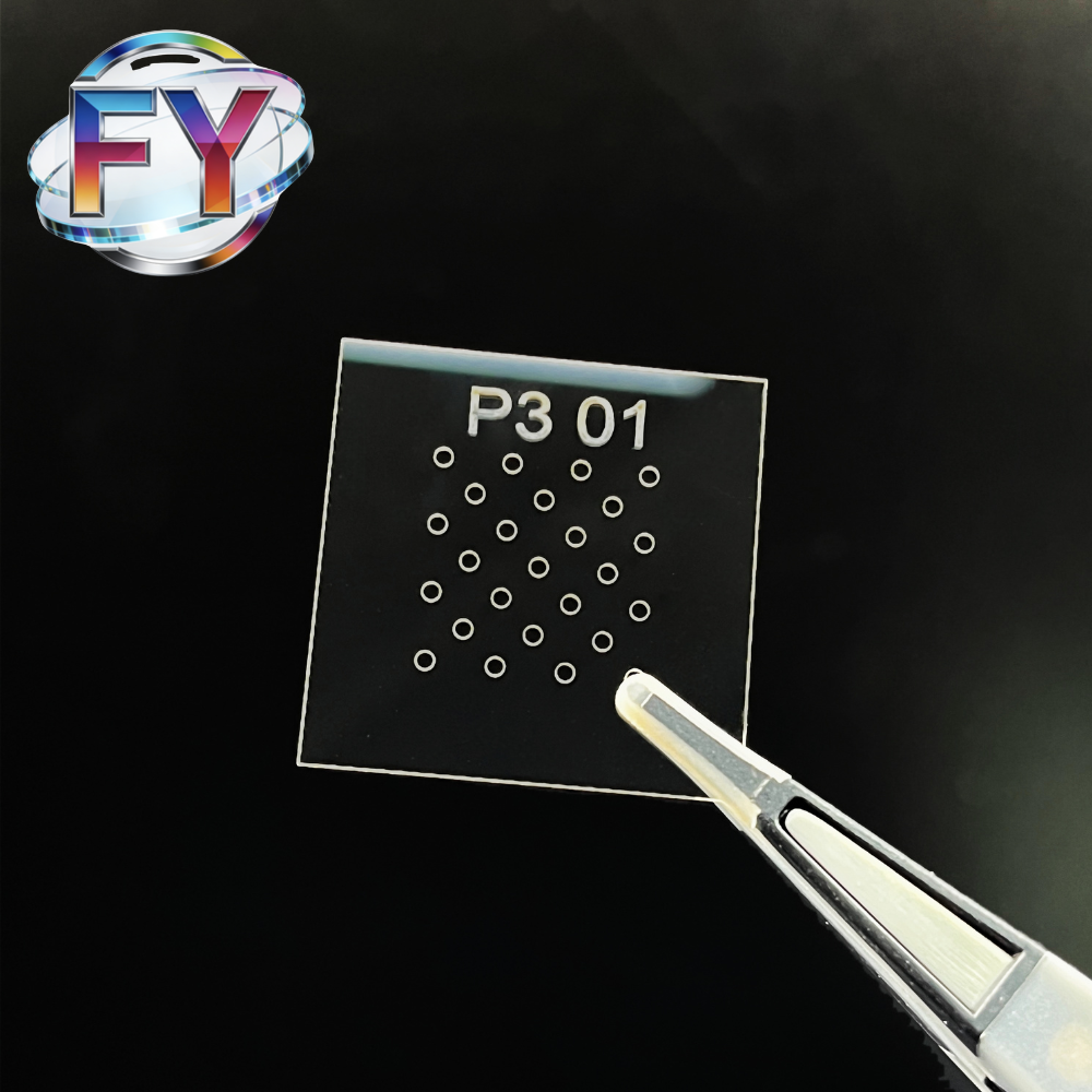
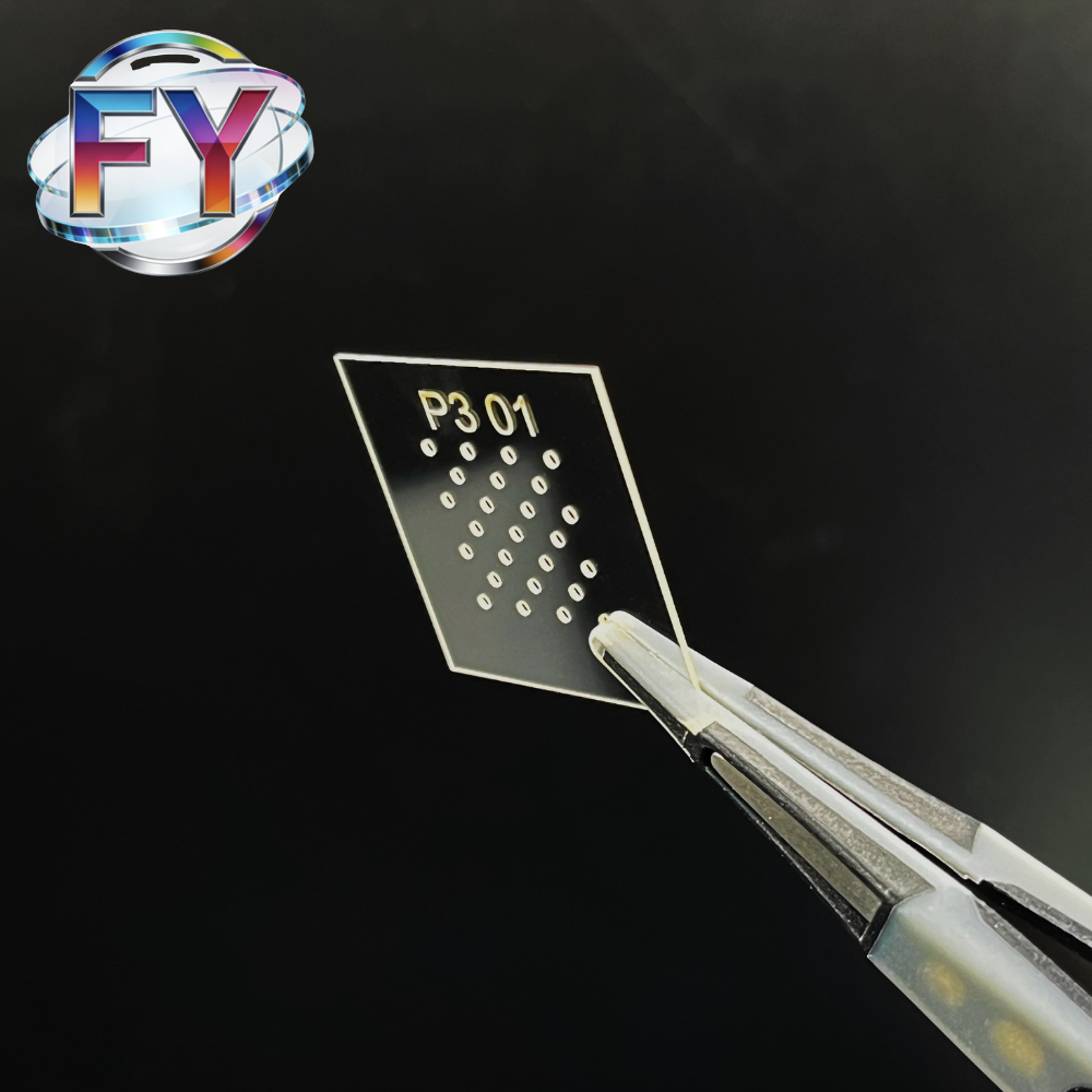
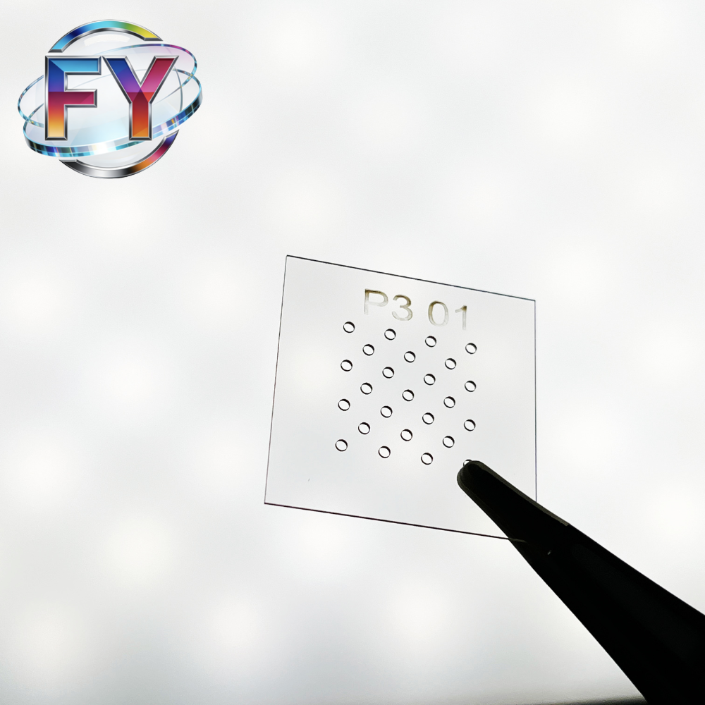
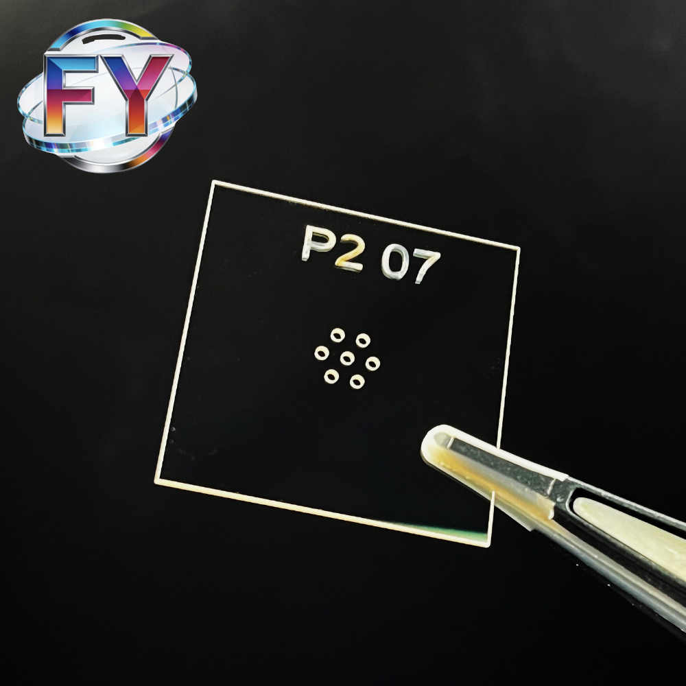
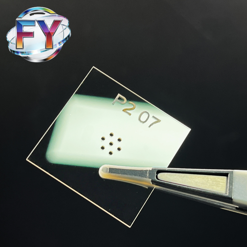
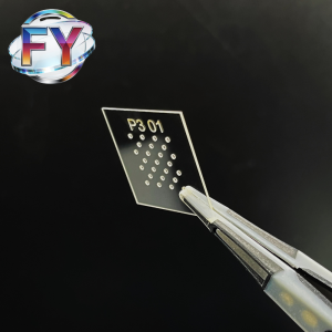
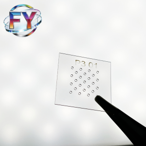
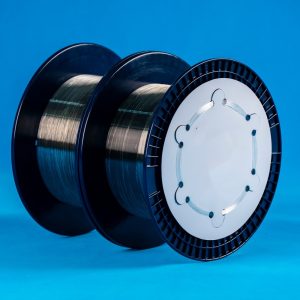
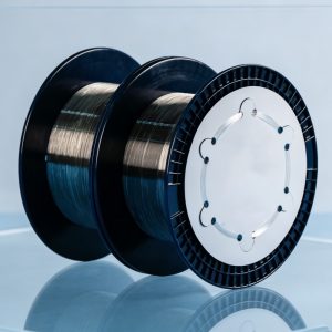
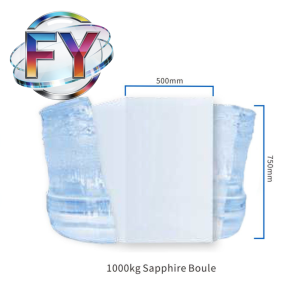
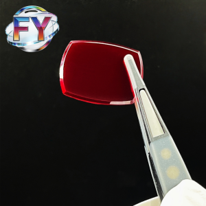
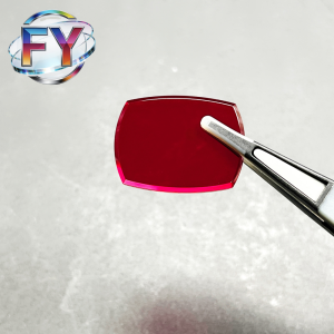
 The Sapphire Through Glass Via (TGV) Substrate is a high-precision microfabricated interposer designed for advanced semiconductor packaging, MEMS devices, and sensor integration. Built on premium Sapphire (Al₂O₃ single crystal) substrates, this technology enables vertical electrical interconnections through ultra-hard, optically transparent, and chemically stable materials.
Compared to traditional silicon or glass interposers, sapphire-based TGV substrates offer superior mechanical strength, higher thermal stability, and enhanced reliability in harsh environments. These advantages make them particularly suitable for high-frequency, high-density, and high-reliability applications such as RF devices, optical sensors, and advanced packaging architectures (2.5D/3D integration).
Key Features & Advantages
1. High-Density Vertical Interconnection
TGV technology enables compact and efficient vertical electrical pathways through sapphire substrates, supporting high-density integration required in modern semiconductor packaging and miniaturized devices.
2. Superior Mechanical Strength
Sapphire’s high hardness (Mohs 9) ensures excellent structural integrity, making the substrate resistant to cracking, warping, and mechanical damage during processing and operation.
3. Excellent High-Frequency Performance
With low dielectric loss, minimal parasitic capacitance, and reduced inductance, sapphire TGV substrates are ideal for RF, 5G, and high-speed signal transmission applications.
4. Outstanding Thermal Stability
Sapphire maintains excellent performance under extreme temperatures, making it suitable for high-power and thermally demanding environments.
5. Chemical Resistance and Hermeticity
The material is highly resistant to acids, alkalis, and corrosive environments. TGV structures can also achieve excellent hermetic sealing performance, ensuring long-term reliability.
6. Optical Transparency
Unlike silicon interposers, sapphire substrates offer optical transparency across UV–IR ranges, enabling integration with optical sensors, photonics, and imaging systems.
Technical Specifications
| Parameter | Specification |
|---|---|
| Product Name | Sapphire TGV Substrate |
| Material | Single-crystal Sapphire (Al₂O₃) |
| Wafer Size | Up to 300 mm |
| Panel Size | Up to 515 × 515 mm |
| Thickness | 0.1 – 0.7 mm (customizable) |
| Min. Thickness | 0.3 mm |
| Via Diameter (OD) | 25 – 100 μm |
| Min. Pitch | ~2 × via diameter |
| Via Type | Through / Blind |
| Via Shape | Straight |
| Aspect Ratio | Up to 1:5 |
| Via Material | Tungsten (W) / Silicon (Si) |
| Hermeticity | ≤ 1×10⁻⁹ Pa·m³/s |
| Tolerance | ±20 μm (per 200 mm wafer) |
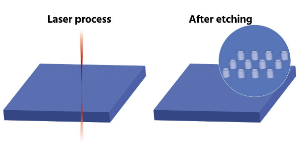 Manufacturing Process
Sapphire TGV substrates are fabricated using advanced laser-induced modification combined with chemical etching:
- Laser Structuring – A precision laser modifies the internal structure of sapphire in predefined via regions
- Selective Etching – Modified regions are etched at faster rates, forming clean, high-aspect-ratio vias
- Metallization – Vias are filled with conductive materials such as tungsten or silicon
- Optional Processes – Including cavity formation, bumping, and surface metallization
This process ensures:
- Crack-free via formation
- High dimensional accuracy
- Smooth via sidewalls
- Compatibility with high-density designs
Applications
Semiconductor Packaging
- 2.5D / 3D interposers
- Wafer-level chip scale packaging (WL-CSP)
- High-density interconnects
MEMS & Sensors
- Pressure sensors
- Optical sensors
- Microfluidic devices
RF & 5G Devices
- High-frequency modules
- Low-loss signal transmission systems
Photonics & Optical Integration
- Optical interposers
- Imaging systems
- Transparent sensor packaging
High-Performance Computing & IoT
- High-bandwidth data transmission
- Compact and high-density integration
Customization Capabilities
We provide fully customizable sapphire TGV solutions tailored to your application requirements:
- Via diameter, pitch, and density optimization
- Wafer or panel-level customization
- Through or blind via design
- Metallization (W, Cu, or custom materials)
- Surface finishing and polishing
- Integration with bonding processes (e.g., anodic bonding)
- High-precision tolerance control
FAQ
Q1: What is the advantage of sapphire TGV over glass or silicon TGV?
A1: Sapphire offers higher mechanical strength, better thermal stability, and optical transparency, making it more suitable for harsh environments and optical-integrated applications.
Q2: Can via size and pitch be customized?
A2: Yes. Via diameter, pitch, and layout can be fully customized according to your design requirements.
Q3: Is sapphire TGV suitable for high-frequency applications?
A3: Absolutely. Its low dielectric loss and excellent electrical properties make it ideal for RF, 5G, and high-speed signal transmission systems.

Reviews
There are no reviews yet.