
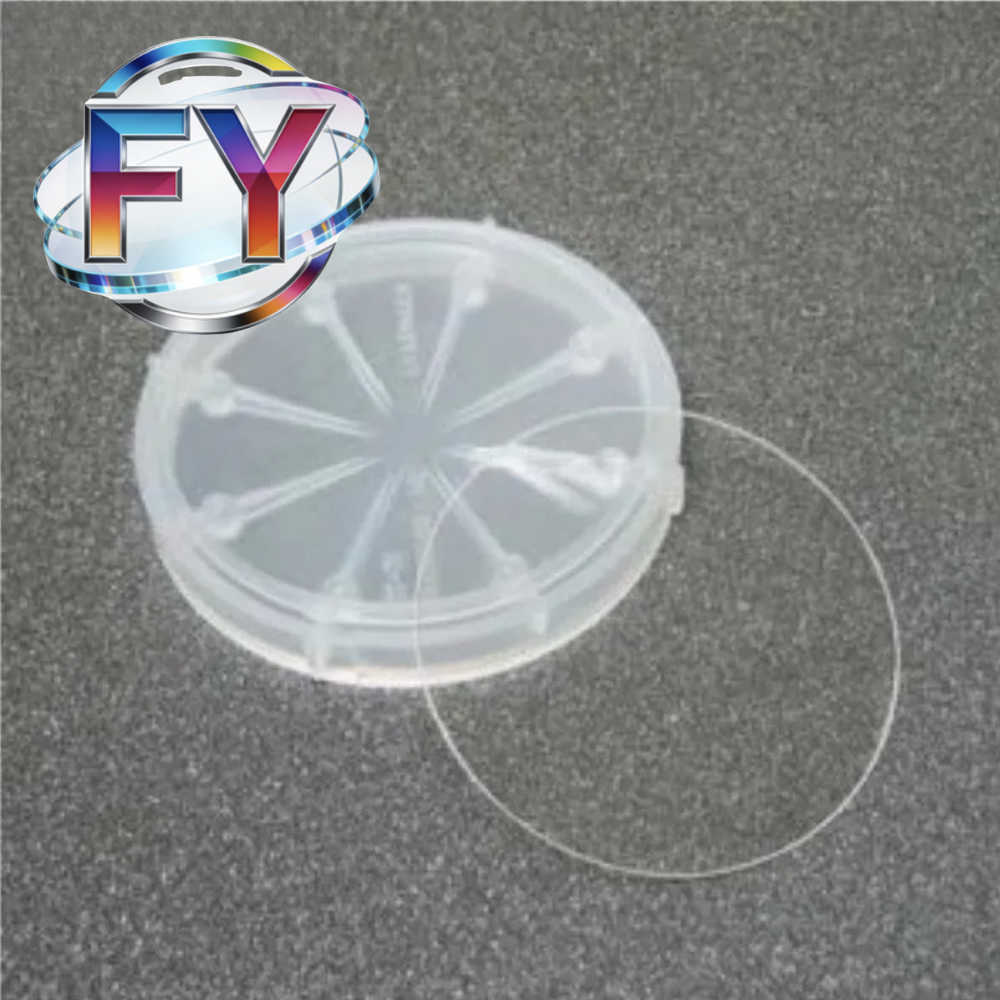
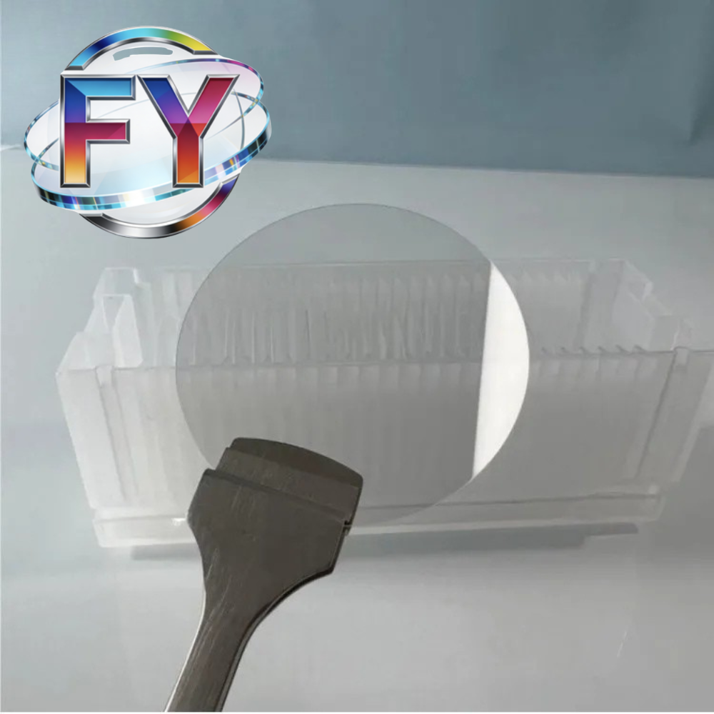

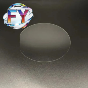
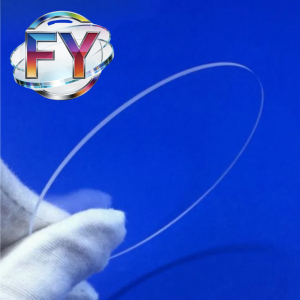
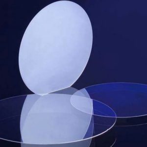
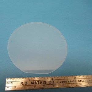
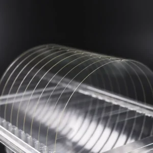
 2palcová křemenná destička je precizně vyrobený substrát z vysoce čistého syntetického taveného křemene. Tato destička se standardním průměrem 50,8 mm nachází široké uplatnění ve výzkumu polovodičů, optickém inženýrství, výrobě MEMS, mikrofluidních zařízeních, vývoji senzorů a pokročilých vědeckých aplikacích. Díky své výjimečné optické průhlednosti, nízkému koeficientu tepelné roztažnosti, vynikající chemické odolnosti a excelentní tepelné stabilitě se křemenné destičky staly důležitým materiálem v odvětvích vyžadujících vysokou přesnost a spolehlivý výkon.
Ve srovnání s běžnými skleněnými substráty se křemenné destičky z taveného křemene vyznačují vyšší čistotou a výrazně lepším výkonem v náročných podmínkách. Díky své schopnosti odolávat vysokým teplotám, chemické korozi a zachovávat rozměrovou stabilitu jsou vhodné jak pro laboratorní výzkum, tak pro průmyslové výrobní procesy. Ať už se používají jako substrát pro nanášení tenkých vrstev, optické povlaky, fotonická zařízení nebo přesné senzory, křemenné destičky poskytují stabilní a spolehlivou platformu pro pokročilé technologie.
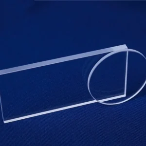
Naše 2palcové křemenné destičky jsou k dispozici v různých kvalitách, včetně materiálů z taveného křemene JGS1, JGS2 a JGS3, což zákazníkům umožňuje vybrat si nejvhodnější optické vlastnosti pro aplikace v ultrafialovém, viditelném nebo infračerveném spektru. Podle konkrétních požadavků projektu lze dodat také rozměry, tloušťky, povrchové úpravy a profily hran na míru.
Specifikace
| Parametr | Specifikace |
|---|---|
| Materiál | Syntetický tavený křemík vysoké čistoty |
| Dostupné ročníky | JGS1 / JGS2 / JGS3 |
| Průměr | 2 palce (50,8 mm) |
| Rozsah tloušťky | 0,1 mm – 3,0 mm |
| Tolerance průměru | ±0,10 mm |
| Povrchová úprava | Leštěné z jedné strany (SSP) / Leštěné z obou stran (DSP) |
| Drsnost povrchu | K dispozici na vyžádání |
| Plochost | K dispozici na vyžádání |
| TTV | K dispozici na vyžádání |
| Typ hrany | Zaoblená hrana / Zkosená hrana |
| Provozní teplota | Až 1000 °C a více |
| Rozsah optického přenosu | 185 nm – 3500 nm |
| Zpracování na zakázku | Vrtání, řezání na kostičky, drážkování, povrchová úprava |
Klíčové vlastnosti
 Vysoká optická propustnost
Tavený křemen je známý svými vynikajícími optickými vlastnostmi v širokém spektru vlnových délek. V závislosti na zvolené kvalitě materiálu mohou křemenné destičky poskytovat vynikající propustnost od hlubokého ultrafialového záření až po infračervené vlnové délky. Díky tomu jsou vhodné pro optická okna, laserové systémy, zobrazovací zařízení, spektroskopické přístroje a fotonická zařízení.
Vynikající tepelná stabilita
Jednou z nejdůležitějších výhod křemenných destiček je jejich mimořádně nízký koeficient tepelné roztažnosti. Díky této vlastnosti si materiál zachovává rozměrovou stabilitu i při teplotních výkyvech a při zpracování za vysokých teplot. Křemenné destičky se proto hojně využívají při výrobě polovodičů, v laboratorních testech a při tepelném zpracování, kde je přesnost zásadní.
Vynikající chemická odolnost
Křemenné destičky vykazují vynikající odolnost vůči většině kyselin, rozpouštědel a korozivních chemikálií. Díky této vlastnosti spolehlivě fungují v náročných výrobních podmínkách i v chemických laboratořích. Jejich chemická stabilita rovněž snižuje riziko kontaminace v citlivých výrobních procesech.
Materiál vysoké čistoty
Tyto destičky, vyrobené ze syntetického taveného křemíku, se vyznačují extrémně nízkým obsahem nečistot a vynikající materiálovou homogenitou. Vysoká čistota je nezbytná pro aplikace v oblasti polovodičů, fotoniky a přesné optiky, kde může kontaminace výrazně ovlivnit výkonnost výrobku.
Přesná kvalita povrchu
Křemenné destičky lze dodávat s jednostranným nebo oboustranným leštěním, aby vyhovovaly různým požadavkům na použití. Vysoce kvalitní leštěné povrchy zlepšují optické vlastnosti, přilnavost povlaků a celkovou konzistenci procesu.
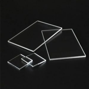
Možnosti zakázkové výroby
Kromě standardních destiček jsou k dispozici i řešení na míru, včetně speciálních tlouštěk, vyvrtaných otvorů, drážek, profilování hran, laserového řezání a optických povlaků. Tato flexibilita umožňuje zákazníkům získat substráty přizpůsobené jejich konkrétním návrhům a výrobním procesům.
Typické aplikace
Výzkum a vývoj v oblasti polovodičů
2palcové křemenné destičky se běžně používají jako substrátové materiály v laboratořích zabývajících se polovodiči a ve výzkumných zařízeních. Díky své tepelné stabilitě a chemické odolnosti jsou vhodné pro nanášení tenkých vrstev, vývoj procesů, výzkum v oblasti balení na úrovni destiček a experimentální výrobu zařízení.
Optické komponenty
Díky vynikající průhlednosti taveného křemene jsou křemenné destičky ideálním materiálem pro výrobu optických součástek. Často se používají v optických okénkách, filtrech, děličích paprsků, krytech senzorů a fotonických zařízeních.
MEMS a mikrosystémy
Mikroelektromechanické systémy vyžadují substráty s vysokou rozměrovou stabilitou a vynikajícími mechanickými vlastnostmi. Křemenné destičky představují spolehlivou platformu pro výrobu MEMS a vývoj zařízení v mikro měřítku.
Mikrofluidní zařízení
Křemenné substráty se stále častěji používají v mikrofluidních čipech pro biomedicínskou diagnostiku, chemickou analýzu a systémy typu „laboratoř na čipu“. Jejich chemická inertnost pomáhá předcházet kontaminaci a zajišťuje přesné výsledky testů.
Senzory a vědecké přístroje
Mnoho moderních senzorů a analytických přístrojů využívá křemenné substráty díky jejich optické průzračnosti, tepelné odolnosti a stabilitě. Mezi jejich aplikace patří tlakové senzory, zařízení pro monitorování životního prostředí, optické senzory a přístroje pro vědecký výzkum.
Laserový a fotonický průmysl
Křemenné destičky se hojně využívají v laserových systémech a fotonických aplikacích, kde je vyžadována vysoká optická propustnost a tepelná odolnost. Mohou sloužit jako základní materiál pro optické povlaky a specializované fotonické struktury.
Dostupné možnosti přizpůsobení
 Nabízíme komplexní služby v oblasti přizpůsobení křemíkových destiček, včetně:
- Leštěná z jedné strany (SSP)
- Oboustranně leštěné (DSP)
- Ultratenké křemíkové destičky
- Silné křemenné podklady
- Křemíkové destičky s průchozími otvory
- Vzorované křemenné substráty
- Povlak AR
- Křemen pro UV použití
- Vlastní tvary
- Řezání laserem
- Přesné řezání na kostky
- Broušení hran a zkosení
Náš tým inženýrů je schopen vyrábět křemenné destičky podle výkresů a technických požadavků zákazníků, a to jak pro vývoj prototypů, tak pro sériovou výrobu.
ČASTO KLADENÉ DOTAZY
Jaká je standardní velikost 2-palcového křemenného plátku?
Standardní průměr 2palcové křemenné destičky je 50,8 mm. Tloušťka se může lišit v závislosti na konkrétním použití, přičemž běžné hodnoty se pohybují v rozmezí od 0,3 mm do 1,0 mm.
Jaký je rozdíl mezi křemennými destičkami JGS1, JGS2 a JGS3?
JGS1 je optimalizován pro propustnost ultrafialového záření, JGS2 se běžně používá pro aplikace ve viditelném spektru a JGS3 je určen pro infračervené optické systémy. Výběr vhodného typu závisí na provozním vlnovém rozsahu.
Je možné dodat křemenné destičky s oboustranným leštěním?
Ano. K dispozici jsou křemenné destičky typu SSP i DSP. Oboustranné leštění se doporučuje pro aplikace vyžadující vysokou rovinnost, vynikající optickou kvalitu nebo přesné procesy nanášení povlaků.
Můžete zajistit rozměry na míru a speciální obrábění?
Ano. Na přání zákazníka lze vyrobit produkty s nestandardní tloušťkou, s vyvrtanými otvory, drážkami, se speciální úpravou hran, s optickými povlaky i v nestandardních tvarech.
Recenze
Zatím zde nejsou žádné recenze.