
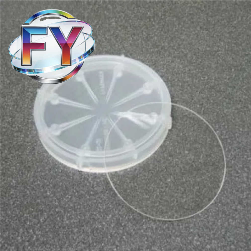
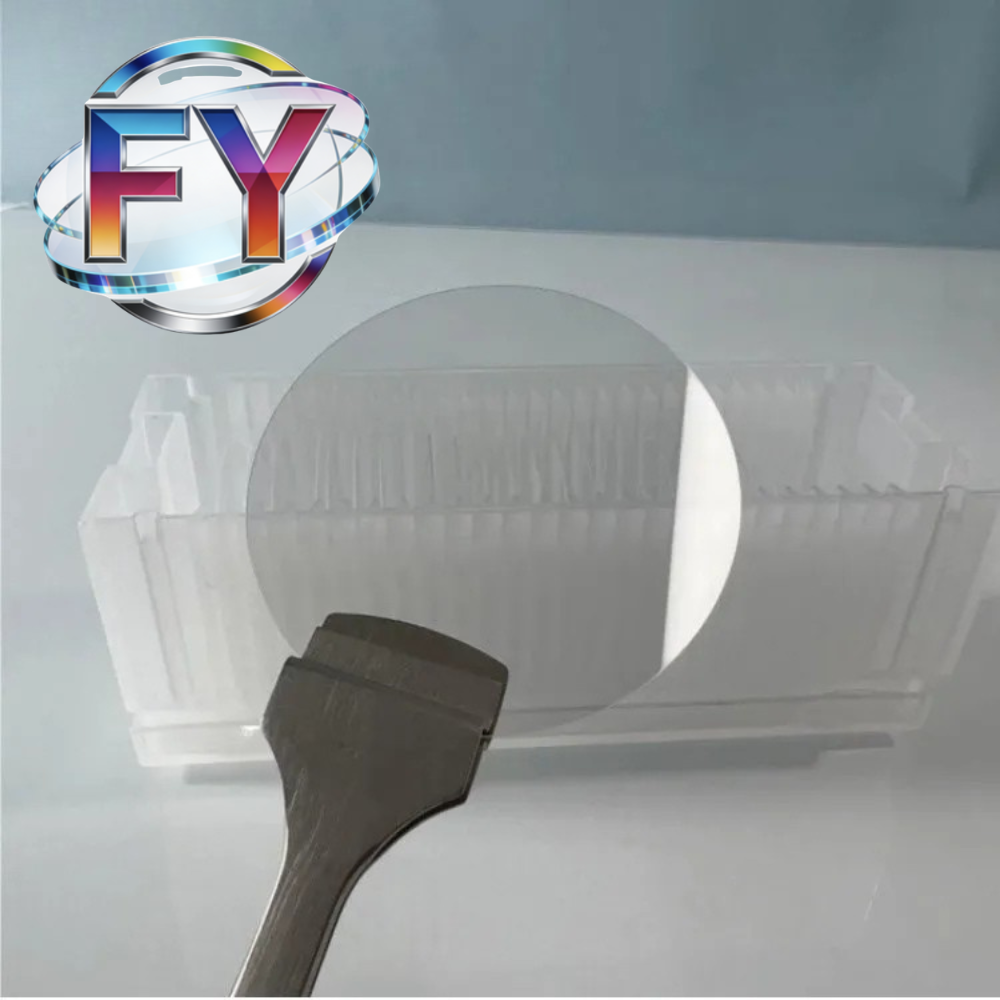

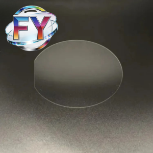
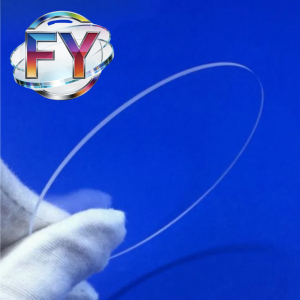
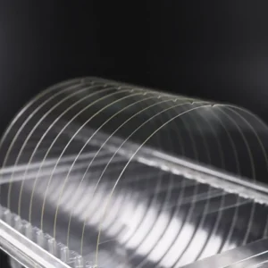
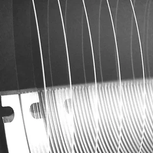
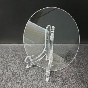
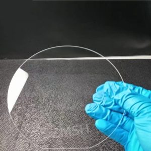
 The 2 Inch Quartz Wafer is a precision-engineered substrate manufactured from high-purity synthetic fused silica. With a standard diameter of 50.8 mm, this wafer is widely used in semiconductor research, optical engineering, MEMS fabrication, microfluidic devices, sensor development, and advanced scientific applications. Thanks to its exceptional optical transparency, low thermal expansion coefficient, outstanding chemical resistance, and excellent thermal stability, quartz wafers have become an important material in industries requiring high precision and reliable performance.
Compared with conventional glass substrates, fused silica quartz wafers offer superior purity and significantly improved performance in demanding environments. Their ability to withstand high temperatures, resist chemical corrosion, and maintain dimensional stability makes them suitable for both laboratory research and industrial production processes. Whether used as a substrate for thin-film deposition, optical coatings, photonic devices, or precision sensors, quartz wafers provide a stable and reliable platform for advanced technologies.
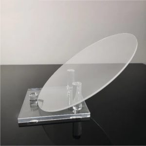
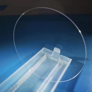
Our 2 inch quartz wafers are available in a variety of grades, including JGS1, JGS2, and JGS3 fused silica materials, allowing customers to select the most suitable optical properties for ultraviolet, visible, or infrared applications. Custom dimensions, thicknesses, surface finishes, and edge profiles can also be supplied according to specific project requirements.
規格
| 參數 | 規格 |
|---|---|
| 材質 | High Purity Synthetic Fused Silica |
| Available Grades | JGS1 / JGS2 / JGS3 |
| 直徑 | 2 Inch (50.8 mm) |
| 厚度範圍 | 0.1 mm – 3.0 mm |
| Diameter Tolerance | ±0.10 mm |
| 表面處理 | Single Side Polished (SSP) / Double Side Polished (DSP) |
| 表面粗糙度 | 可依需求提供 |
| 平整度 | 可依需求提供 |
| TTV | 可依需求提供 |
| 邊緣類型 | Rounded Edge / Chamfered Edge |
| 操作溫度 | Up to 1000°C+ |
| 光學傳輸範圍 | 185 nm – 3500 nm |
| Custom Processing | Drilling, Dicing, Slotting, Coating |
主要功能
 High Optical Transmission
Fused silica is recognized for its excellent optical performance across a broad wavelength range. Depending on the selected material grade, quartz wafers can provide outstanding transmission from deep ultraviolet to infrared wavelengths. This makes them suitable for optical windows, laser systems, imaging equipment, spectroscopy instruments, and photonic devices.
優異的熱穩定性
One of the most important advantages of quartz wafers is their extremely low coefficient of thermal expansion. This characteristic allows the material to maintain dimensional stability during temperature fluctuations and high-temperature processing. As a result, quartz wafers are widely used in semiconductor manufacturing, laboratory testing, and thermal processing applications where precision is critical.
Superior Chemical Resistance
Quartz wafers exhibit excellent resistance to most acids, solvents, and corrosive chemicals. This property allows them to perform reliably in harsh processing environments and chemical laboratories. Their chemical stability also reduces contamination risks in sensitive manufacturing processes.
High Purity Material
Manufactured from synthetic fused silica, these wafers offer extremely low impurity levels and excellent material consistency. High purity is essential for semiconductor, photonics, and precision optical applications where contamination can significantly affect product performance.
精密表面品質
Quartz wafers can be supplied with single-side polishing or double-side polishing to meet different application requirements. High-quality polished surfaces improve optical performance, coating adhesion, and overall process consistency.
Custom Manufacturing Capabilities
In addition to standard wafers, custom solutions are available, including special thicknesses, drilled holes, slots, edge profiling, laser cutting, and optical coatings. This flexibility enables customers to obtain substrates tailored to their specific designs and manufacturing processes.
典型應用
Semiconductor Research and Development
2 inch quartz wafers are commonly used as substrate materials in semiconductor laboratories and research facilities. Their thermal stability and chemical resistance make them suitable for thin-film deposition, process development, wafer-level packaging studies, and experimental device fabrication.
光學元件
The excellent transparency of fused silica makes quartz wafers an ideal material for manufacturing optical components. They are frequently used in optical windows, filters, beam splitters, sensor covers, and photonic devices.
MEMS and Microsystems
Micro-electromechanical systems require substrates with high dimensional stability and excellent mechanical properties. Quartz wafers provide a reliable platform for MEMS fabrication and micro-scale device development.
微流體裝置
Quartz substrates are increasingly used in microfluidic chips for biomedical diagnostics, chemical analysis, and laboratory-on-chip systems. Their chemical inertness helps prevent contamination and ensures accurate testing results.
Sensors and Scientific Instruments
Many advanced sensors and analytical instruments rely on quartz substrates due to their optical clarity, thermal resistance, and stability. Applications include pressure sensors, environmental monitoring equipment, optical sensors, and scientific research instruments.
Laser and Photonics Industry
Quartz wafers are widely utilized in laser systems and photonics applications where high optical transmission and thermal durability are required. They can serve as base materials for optical coatings and specialized photonic structures.
Available Custom Options
 We provide comprehensive customization services for quartz wafers, including:
- Single Side Polished (SSP)
- Double Side Polished (DSP)
- Ultra-Thin Quartz Wafers
- Thick Quartz Substrates
- Through-Hole Quartz Wafers
- Patterned Quartz Substrates
- AR 塗層
- UV Grade Quartz
- Custom Shapes
- 雷射切割
- Precision Dicing
- Edge Grinding and Chamfering
Our engineering team can manufacture quartz wafers according to customer drawings and technical requirements, supporting both prototype development and volume production.
常見問題
What is the standard size of a 2 inch quartz wafer?
The standard diameter of a 2 inch quartz wafer is 50.8 mm. Thicknesses can vary depending on the application, with common options ranging from 0.3 mm to 1.0 mm.
What is the difference between JGS1, JGS2, and JGS3 quartz wafers?
JGS1 is optimized for ultraviolet transmission, JGS2 is commonly used for visible light applications, and JGS3 is designed for infrared optical systems. The appropriate grade depends on the operating wavelength range.
Can quartz wafers be supplied with double-side polishing?
Yes. Both SSP and DSP quartz wafers are available. Double-side polishing is recommended for applications requiring high flatness, superior optical quality, or precision coating processes.
Can you provide custom dimensions and special machining?
Yes. Custom thicknesses, drilled holes, slots, special edge treatments, optical coatings, and non-standard shapes can all be manufactured according to customer specifications.
商品評價
目前沒有評價。