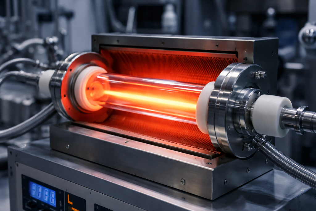
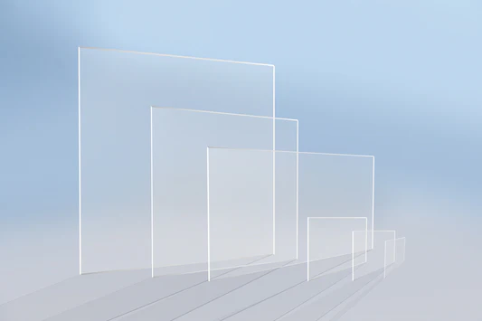
Glass wafers are widely used in MEMS, microfluidics, wafer-level packaging, sensors and semiconductor R&D.
Among the available glass materials, BOROFLOAT® 33 borosilicate glass is particularly well known because its thermal expansion behavior is relatively well matched to silicon and because its alkali-containing composition enables anodic bonding.
Typical applications include:
- MEMS pressure sensors;
- accelerometers;
- gyroscopes;
- microfluidic devices;
- silicon-glass cavity sealing;
- wafer-level packaging;
- optical MEMS;
- lab-on-chip devices;
- wafer-level optics;
- temporary carrier wafers;
- structured glass substrates.
However, simply specifying:
BF33 glass wafer
is usually not enough for a production RFQ.
For wafer-level processing, engineers should also define:
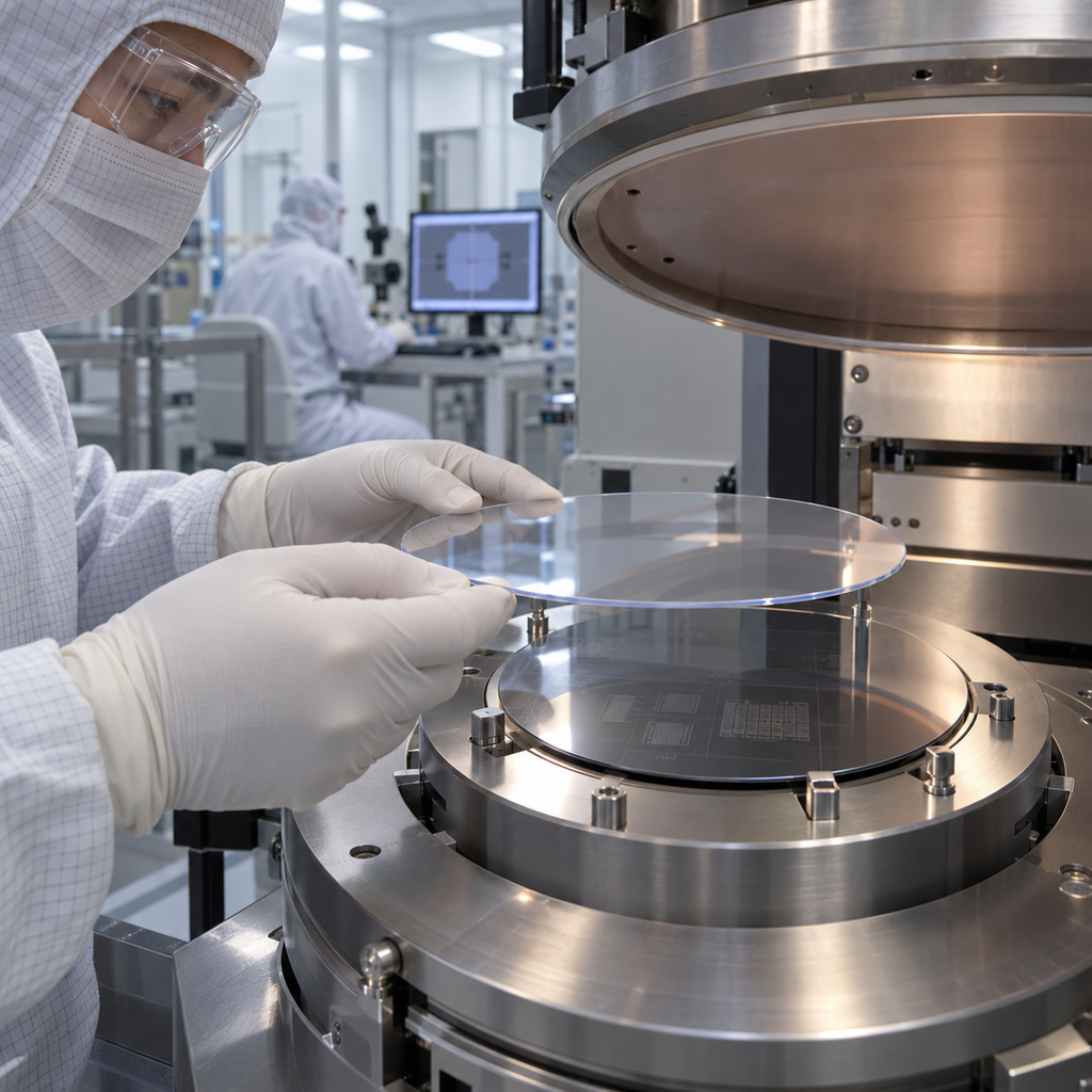
diameter → thickness → thickness tolerance → TTV → bow/warp → surface roughness → scratch-dig → edge profile → flat/notch → holes/cavities → bonding process
These parameters can determine whether the glass wafer can be successfully aligned, bonded and processed with the silicon wafer.
This guide explains how to specify BF33 / BOROFLOAT® 33 glass wafers for MEMS and anodic bonding.
1. What Is BOROFLOAT® 33?
BOROFLOAT® 33 is a borosilicate glass manufactured by SCHOTT using a microfloat process.
It should not be confused with fused silica.
The two materials have significantly different compositions and thermal properties.
BOROFLOAT® 33 contains boron oxide and alkali components in addition to silica, while fused silica consists predominantly of SiO₂.
A major characteristic of BOROFLOAT® 33 is its coefficient of thermal expansion.
SCHOTT specifies its mean linear CTE as approximately:
3.25 × 10⁻⁶ K⁻¹ from 20°C to 300°C.
Other published properties include approximately:
- transformation temperature Tg: 525°C
- thermal conductivity at 90°C: 1.2 W/(m·K)
- density: 2.23 g/cm³
- Young’s modulus: approximately 64 GPa
- refractive index nd: approximately 1.4714.
This combination of thermal, optical, electrical and chemical properties makes it useful for silicon-glass microsystems.
2. BF33 Is Not Fused Silica
This distinction is important for both design and purchasing.
A customer may sometimes request:
Quartz glass wafer, BF33.
Technically, this mixes two different material families.
A simplified comparison is:
| Property | BF33 / BOROFLOAT® 33 | Fused Silica |
|---|---|---|
| Material family | Borosilicate glass | High-silica amorphous SiO₂ |
| CTE | ~3.25 × 10⁻⁶/K | ~0.5 × 10⁻⁶/K |
| Alkali content | Present | Extremely low in high-purity grades |
| Anodic bonding to Si | Excellent application fit | More difficult without suitable mobile ions/process modification |
| Thermal shock | Very good | Excellent |
| Deep UV performance | Limited compared with UV fused silica | Excellent in suitable grades |
| Typical MEMS use | Very common | Application dependent |
| Relative material cost | Usually lower | Usually higher |
Therefore:
BF33 is not a lower-cost grade of fused silica.
It is a different glass engineered for different applications.
3. Why BOROFLOAT 33 Is Used for Silicon Anodic Bonding
Anodic bonding—also called electrostatic or field-assisted bonding—is widely used to join silicon to alkali-containing glass.
The process typically uses:
- elevated temperature;
- high electric field;
- intimate surface contact.
Under the electric field, mobile alkali ions in the glass migrate away from the silicon-glass interface.
This creates a depletion region and strong electrostatic attraction between the surfaces, eventually producing a stable chemical bond.
Borosilicate glasses such as BOROFLOAT® have long been among the most commonly used materials for this process.
SCHOTT also specifically identifies BOROFLOAT® 33 as suitable for anodic bonding because its thermal expansion behavior corresponds closely with silicon over the relevant temperature range.
4. Why CTE Matching Matters
During anodic bonding, the silicon and glass stack is heated and later cooled to room temperature.
If the two materials expand and contract at very different rates, residual stress develops after bonding.
This can cause:
- wafer bow;
- local deformation;
- interface stress;
- fracture;
- MEMS diaphragm distortion;
- cavity deformation;
- sensor offset;
- long-term reliability problems.
For a bonded wafer pair, thermal mismatch strain can be approximated conceptually as:
Δε ≈ (αglass − αSi) × ΔT
where:
- αglass = glass CTE;
- αSi = silicon CTE;
- ΔT = temperature change.
The closer the thermal expansion behavior of the two substrates, the lower the potential thermal mismatch stress.
This is one reason borosilicate glasses with CTE around 3.2–3.3 × 10⁻⁶/K are widely used with silicon.
The important point is that silicon CTE itself varies with temperature, so “CTE matching” should be evaluated over the actual bonding and operating temperature range rather than comparing one room-temperature number.
5. Typical Applications in MEMS
BOROFLOAT® 33 glass wafers are frequently used for several functions within MEMS devices.
Cavity Cap
A glass wafer can be bonded over a micromachined silicon wafer to create a sealed cavity.
Applications include:
- pressure sensors;
- resonators;
- accelerometers;
- gyroscopes.
Transparent Cover
Because the glass is optically transparent, it can provide optical access to:
- mirrors;
- microchannels;
- optical MEMS;
- sensors.
Mechanical Substrate
The glass can support silicon structures or electronic assemblies.
Microfluidic Layer
Channels, holes and chambers can be machined into the glass before bonding.
Wafer-Level Packaging
An entire silicon wafer can be capped before dicing.
This allows hundreds or thousands of devices to be packaged simultaneously.
6. Glass Wafer Diameter
Common custom wafer diameters include:
- 2 inch;
- 3 inch;
- 4 inch / 100 mm;
- 5 inch;
- 6 inch / 150 mm;
- 8 inch / 200 mm;
- 12 inch / 300 mm.
SCHOTT’s current processed glass-carrier portfolio includes wafer formats from 150 mm through 300 mm, including 6-, 8- and 12-inch formats.
Smaller custom diameters can also be machined from sheet material.
For an RFQ, diameter should ideally include tolerance:
Ø100.00 ± 0.10 mm
rather than simply:
4-inch glass wafer.
7. Raw BOROFLOAT Sheet vs Precision Glass Wafer
This is one of the most important distinctions for buyers.
Commercial BOROFLOAT® 33 is available as float sheet glass in many thicknesses.
For example, SCHOTT lists standard sheet thicknesses including:
0.70, 1.10, 1.75, 2.00, 2.25, 2.75, 3.30 mm
and substantially thicker sheet formats.
But the thickness tolerance of raw float sheet is not the same as the thickness tolerance expected from a precision semiconductor wafer.
For example, standard 0.70 mm BOROFLOAT sheet is listed at approximately:
0.70 ± 0.05 mm
That is ±50 µm.
For precision wafer processing, this may be far too loose.
The wafer may therefore require:
cutting → edge grinding → lapping → polishing → thickness control → TTV inspection
before it is suitable for advanced MEMS bonding.
8. Thickness Options for Precision Wafer Processing
Typical finished glass-wafer thicknesses may include:
- 200 µm;
- 300 µm;
- 400 µm;
- 500 µm;
- 700 µm;
- 1.0 mm;
- 1.1 mm;
- 2.0 mm;
- 3.0 mm.
Current SCHOTT carrier-wafer specifications list BOROFLOAT® 33 wafer thicknesses approximately from:
0.4 mm to 3.0 mm
for processed wafer formats.
Structured-glass processing can cover even broader thickness ranges depending on the manufacturing route; SCHOTT reports structured glass capabilities from approximately 0.1 to 3.3 mm for selected glass types.
For custom fabrication, feasibility depends on:
- diameter;
- required TTV;
- surface finish;
- final bow/warp;
- mechanical strength.
Very thin large-diameter glass wafers become progressively more difficult to handle.
9. Thickness Tolerance vs TTV
These two specifications are often confused.
They are not the same.
Thickness Tolerance
Thickness tolerance defines how close the wafer’s average or center thickness must be to the nominal value.
Example:
500 ± 10 µm
TTV — Total Thickness Variation
TTV measures the difference between the maximum and minimum wafer thickness.
For example:
- thickest point = 502 µm;
- thinnest point = 497 µm.
Then:
TTV = 5 µm
A wafer could theoretically meet its average thickness specification but still have excessive TTV.
For wafer bonding and lithography, TTV can be more important than nominal thickness.
10. Why TTV Matters in MEMS
Excessive TTV can create problems during:
- anodic bonding;
- lithography;
- coating;
- wafer chucking;
- cavity formation;
- wafer-level packaging;
- alignment.
If the glass thickness varies significantly across the wafer, some regions may contact the silicon earlier than others during bonding.
This can increase the risk of:
- trapped gas;
- incomplete bonding;
- local stress;
- bond-front irregularity.
For precision MEMS structures, thickness variation can also influence final cavity dimensions.
11. What TTV Can Be Achieved?
TTV depends heavily on whether the buyer is purchasing:
raw float glass
or:
precision processed glass wafers.
Current SCHOTT specifications for precision glass carrier wafers list:
Standard TTV: ≤2.0 µm
and:
Advanced TTV: ≤0.5 µm
for selected glass wafer products.
The same data list precision thickness tolerances around:
±5 µm standard
and:
±2.5 µm advanced
for processed wafer products.
These values should not be interpreted as the default specification for every BOROFLOAT wafer.
They demonstrate what can be achieved with precision wafer processing.
For many MEMS projects, specifications such as:
TTV ≤10 µm
or:
TTV ≤5 µm
may already be sufficient and more economical.
The tolerance should therefore be driven by the process.
12. Do Not Overspecify TTV
A common RFQ mistake is requesting:
TTV ≤1 µm
without confirming whether the process actually requires it.
Tighter TTV generally means:
- more lapping;
- more polishing;
- additional metrology;
- lower manufacturing yield;
- higher cost.
For a simple microfluidic cover wafer, TTV ≤10 or 20 µm may potentially be sufficient.
For precision wafer-to-wafer MEMS bonding, much tighter values may be justified.
The correct question is:
What TTV can the bonding and lithography process tolerate?
not:
What is the lowest TTV available?
13. Surface Roughness for Anodic Bonding
Bonding surfaces must be sufficiently smooth and clean for intimate contact.
Important surface parameters include:
- Ra;
- RMS roughness;
- waviness;
- scratches;
- pits;
- particles.
Commercial structured BOROFLOAT® wafer processes can achieve surface roughness around:
Ra ≤1.5 nm
for appropriate products.
However, the actual roughness required depends on:
- bonding temperature;
- voltage;
- surface cleaning;
- local flatness;
- cavity structure.
A typical precision RFQ might specify:
Ra ≤1 nm
or:
Ra ≤1.5 nm
for the bonding surface.
Do not specify nanometer-level roughness for both sides unless both surfaces require it.
14. Single-Side vs Double-Side Polished
Glass wafers can be supplied as:
Single-Side Polished — SSP
One side receives the primary precision polishing treatment.
Suitable when only one side will be used for:
- bonding;
- optical access;
- coating.
Double-Side Polished — DSP
Both surfaces are polished.
DSP wafers are preferable when:
- both sides require lithography;
- both sides require optical quality;
- front-to-back alignment is needed;
- very low TTV is required;
- the wafer will undergo multiple bonding steps.
For MEMS wafer-level processing, DSP is often requested.
15. Surface Quality: Scratch and Dig
Optical or transparent MEMS devices may also specify surface quality using scratch-dig notation.
Examples include:
60/40
40/20
20/10
The correct requirement depends on whether the glass functions primarily as:
- mechanical package;
- bonding substrate;
- optical window.
Current SCHOTT glass-carrier data list:
40/20 standard
and:
20/10 advanced
surface cosmetic quality for selected precision wafer products.
For purely mechanical MEMS bonding, specifying 10/5 optical quality may add unnecessary cost.
16. Bow and Warp
TTV describes thickness variation.
Bow and warp describe wafer shape.
A glass wafer can have excellent TTV but still be curved.
Excessive wafer deformation can cause:
- chucking problems;
- robot handling issues;
- lithography focus problems;
- incomplete bonding;
- alignment errors.
Current SCHOTT processed carrier-wafer data provide examples of wafer-level warp capability, including approximately:
- ≤30 µm for selected 8-inch wafer configurations
- ≤50 µm for selected 12-inch configurations
under the published specification.
Actual requirements should be defined according to wafer size and bonding equipment.
17. Flatness Is Especially Important Around Bonding Areas
Global bow does not fully describe local bonding quality.
For MEMS devices with many small cavities, local surface condition around the bonding frames may determine whether a hermetic seal can be formed.
Important defects include:
- local pits;
- particles;
- scratches;
- edge roll-off;
- waviness.
A wafer can therefore pass global thickness measurements and still fail bonding because of localized surface defects.
This is why cleaning and surface inspection are as important as dimensional metrology.
18. Glass Wafer Edge Profile
Finished semiconductor-style glass wafers normally require an engineered edge.
Options include:
- rounded edge;
- bevel;
- chamfer;
- ground edge;
- polished edge.
A sharp laser- or mechanically-cut edge increases:
- chipping;
- crack initiation;
- particle generation;
- handling damage.
For automated wafer handling, specify:
- diameter;
- bevel profile;
- notch or flat;
- edge-chipping limit.
This becomes increasingly important at 200 and 300 mm.
19. Flat and Notch Options
Custom BF33 glass wafers can be supplied with:
- no orientation feature;
- one flat;
- two flats;
- notch.
For MEMS production, the orientation feature may be used by equipment for:
- alignment;
- wafer mapping;
- process orientation;
- robot handling.
Glass itself does not require a crystallographic orientation like silicon.
However, the flat or notch may need to match the orientation of the corresponding silicon wafer.
Therefore an RFQ should state:
Notch position relative to silicon device layout
when alignment matters.
20. Structured BF33 Glass Wafers
Many MEMS projects require more than a blank glass disc.
Glass wafers may include:
- through holes;
- cavities;
- channels;
- counterbores;
- slots;
- alignment marks;
- recesses;
- vias.
These structures can be produced by methods such as:
- ultrasonic machining;
- laser processing;
- abrasive processes;
- wet etching;
- precision grinding.
SCHOTT’s structured wafer capability, for example, lists through-structure feature tolerances below approximately 20 µm total, position tolerances below approximately 20 µm, and structured wafers up to large formats depending on design.
Actual achievable tolerances depend strongly on:
- feature size;
- wafer thickness;
- hole count;
- edge distance;
- glass type.
21. Through Holes for MEMS Packaging
Through holes may be used for:
- pressure access;
- fluid inlet/outlet;
- electrical feedthroughs;
- alignment;
- vacuum communication.
An RFQ should specify:
hole diameter
hole tolerance
position tolerance
taper
entrance/exit chipping
quantity per wafer
For example:
50 holes, Ø500 ±20 µm, position ±25 µm.
This is substantially more useful than:
Need drilled BF33 wafer.
22. BF33 for Microfluidics
Borosilicate glass is also attractive for microfluidic devices because of its:
- optical transparency;
- chemical resistance;
- dimensional stability;
- compatibility with structured channels;
- ability to bond with silicon.
Applications include:
- chemical analysis;
- biomedical diagnostics;
- flow sensors;
- lab-on-chip;
- microreactors.
If the wafer contains microfluidic channels, the RFQ should additionally define:
- channel depth;
- channel width;
- sidewall profile;
- surface roughness;
- inlet/outlet geometry.
23. BOROFLOAT 33 for Wafer-Level Packaging
MEMS devices often need hermetic protection.
Glass caps offer several advantages:
- optical transparency;
- wafer-level processing;
- cavity formation;
- compatibility with anodic bonding.
SCHOTT also uses BOROFLOAT® 33 in wafer-level MEMS packaging products incorporating hermetic through-glass vias, demonstrating the material’s compatibility with silicon bonding and miniaturized packages.
Potential devices include:
- microphones;
- pressure sensors;
- inertial sensors;
- optical MEMS;
- resonators.
24. Anodic Bonding Surface Preparation
Even excellent glass will not bond properly if the surface is contaminated.
Before bonding, surfaces generally need careful cleaning to remove:
- organic residue;
- particles;
- metals;
- polishing residue.
The actual cleaning recipe depends on device compatibility.
Common semiconductor cleaning strategies may involve:
- DI-water cleaning;
- solvent cleaning;
- plasma treatment;
- RCA-type processes;
- specialized glass cleaning.
The goal is to achieve:
clean + smooth + particle-free + sufficiently flat surfaces
before applying heat and voltage.
25. Bonding Temperature and Voltage
Anodic bonding is a process window rather than one universal temperature/voltage recipe.
Bond performance depends on:
- glass composition;
- wafer thickness;
- device structure;
- temperature;
- applied voltage;
- bonding time;
- surface condition.
Published engineering references describe anodic bonding as a relatively low-temperature electrochemical bonding process that requires elevated temperature and a strong electric field.
For a production process, bonding parameters should be optimized experimentally.
A material supplier should therefore avoid promising:
BF33 always bonds at X°C and Y volts.
Actual conditions belong to the bonding process, not simply to the glass datasheet.
26. Why Thickness Matters During Anodic Bonding
Glass thickness affects several aspects of the process.
A thicker wafer may provide:
- greater stiffness;
- better mechanical protection;
- deeper cavities.
But it can also influence:
- electric-field distribution;
- thermal mass;
- device thickness;
- optical path.
A thin wafer provides:
- lower package height;
- potentially easier optical integration.
But it is more sensitive to:
- handling;
- bow;
- breakage.
Therefore thickness should be selected according to the final device—not simply based on available stock.
27. 4-Inch vs 6-Inch vs 8-Inch BF33 Wafers
Moving to larger glass wafers increases process productivity because more devices can be fabricated simultaneously.
However, larger diameter increases the importance of:
- TTV;
- bow;
- warp;
- edge integrity;
- handling.
100 mm / 4 inch
Common for:
- universities;
- MEMS R&D;
- small production lines.
150 mm / 6 inch
Widely used for:
- MEMS manufacturing;
- sensors;
- microfluidics.
200 mm / 8 inch
Increasingly relevant to higher-volume MEMS and wafer-level packaging.
300 mm / 12 inch
Used for selected advanced semiconductor, carrier and wafer-level applications.
As diameter increases, specifications should generally become more process-driven.
28. Custom Sizes
Not every project requires a standard SEMI wafer diameter.
Custom options can include:
- round discs;
- square substrates;
- rectangular plates;
- custom-diameter wafers;
- wafers with cutouts.
Large BOROFLOAT® sheet material can be processed into many custom dimensions. SCHOTT’s base sheet portfolio itself covers panel sizes substantially larger than standard semiconductor wafers.
This makes BF33 useful for both:
wafer-level applications
and:
panel-level development.
29. BF33 vs Fused Silica for MEMS
Which material should a customer select?
Choose BF33 / Borosilicate Glass When:
- anodic bonding with silicon is required;
- CTE matching to silicon is important;
- moderate-to-high temperature resistance is sufficient;
- cost matters;
- optical transparency is required;
- mobile alkali ions are beneficial for bonding.
Consider Fused Silica When:
- ultra-low thermal expansion is required;
- very high chemical purity is required;
- deep-UV transmission matters;
- extremely low alkali content is required;
- semiconductor contamination control is more important than conventional anodic bonding behavior.
The two materials should not be treated as interchangeable.
30. BF33 vs Soda-Lime Glass
Standard soda-lime glass is usually a poor substitute for MEMS anodic bonding when tight thermal matching is required.
BOROFLOAT® 33 has a substantially lower CTE.
SCHOTT reports that its CTE is approximately three times lower than ordinary soda-lime glass.
This reduces thermal mismatch with silicon during bonding and temperature cycling.
Soda-lime glass may be cheaper, but the material saving can be insignificant compared with the cost of:
- failed bonding;
- wafer cracking;
- MEMS offset drift;
- reliability failures.
31. BF33 vs MEMpax
Another material sometimes encountered in MEMS applications is SCHOTT MEMpax®.
Both are borosilicate glasses with thermal expansion suitable for silicon-related applications.
However, they are produced using different manufacturing processes and are available in different thickness and surface-quality ranges.
SCHOTT specifically notes these manufacturing differences while identifying both glass types as suitable for anodic bonding.
Therefore MEMpax should not automatically be treated as simply another trade name for BOROFLOAT 33.
32. Example Specification — 100mm MEMS Glass Wafer
A useful RFQ might read:
Material: BOROFLOAT® 33
Diameter: 100.00 ±0.10 mm
Thickness: 500 ±10 µm
TTV: ≤5 µm
Surface: DSP
Surface Roughness: Ra ≤1 nm
Bow: ≤30 µm
Warp: ≤30 µm
Edge: Beveled
Flat: Required
Surface Quality: 40/20
Application: Si-glass anodic bonding
Quantity: 25 pcs
This gives the supplier substantially more information than:
Need 4-inch BF33 wafer.
33. Example Specification — 200mm Glass Wafer
Material: BF33-type borosilicate glass / BOROFLOAT® 33 if specifically required
Diameter: 200 mm
Thickness: 700 µm
Thickness Tolerance: ±10 µm
TTV: ≤5 µm
Surface: Double-side polished
Ra: ≤1.5 nm
Warp: Customer specified
Notch: SEMI-style/custom orientation
Edge: Rounded bevel
Application: MEMS wafer-level packaging
Quantity: 50 pcs
For high-volume bonding, wafer mapping data can also be discussed.
34. Example RFQ — Structured MEMS Glass Wafer
Material: BOROFLOAT® 33
Diameter: 150 mm
Thickness: 700 µm
TTV: ≤10 µm
Surface: DSP
Structure:
- Through holes: 120 pcs
- Hole diameter: Ø400 µm
- Diameter tolerance: ±20 µm
- Position tolerance: ±25 µm
- Maximum chipping: customer specified
Bonding Side Ra: ≤1 nm
Application: Silicon-glass anodic bonding
Quantity: Prototype 10 pcs / Production 500 pcs
For structured wafers, a drawing in PDF + STEP/DXF format can significantly reduce technical clarification.
35. What Information Should Be Included in a BF33 Wafer RFQ?
For fast evaluation, provide:
Material
- Genuine SCHOTT BOROFLOAT® 33
- BF33-type equivalent allowed/not allowed
- Alternative borosilicate glass allowed/not allowed
Wafer Dimensions
- Diameter
- Thickness
- Diameter tolerance
- Thickness tolerance
Geometry
- TTV
- Bow
- Warp
- Flatness
Surface
- SSP or DSP
- Ra
- Scratch-dig
- Optical requirement if applicable
Edge
- Rounded
- Beveled
- Chamfered
- Flat/notch
Structures
- Holes
- Cavities
- Channels
- Slots
- Counterbores
- Alignment marks
Bonding
- Anodic bonding
- Adhesive bonding
- Fusion bonding
- Temporary bonding
Matching Substrate
- Silicon
- SOI
- Glass
- Other
Quantity
- R&D
- Qualification
- Mass production
This information allows the supplier to determine whether a standard float-glass wafer is sufficient or whether precision lapping and polishing are required.
36. The Most Common Procurement Mistakes
Mistake 1: Specifying Only “BF33”
The glass grade does not define:
- thickness tolerance;
- TTV;
- surface roughness;
- bow;
- edge condition.
Mistake 2: Confusing Raw Sheet Tolerance with Wafer Tolerance
A ±50 µm stock-sheet thickness tolerance is completely different from a ±5 µm precision wafer specification.
Mistake 3: Requesting Extremely Low TTV Without Need
This unnecessarily increases cost.
Mistake 4: Ignoring Bow and Warp
A low-TTV wafer can still create bonding problems if it is badly warped.
Mistake 5: Ignoring Surface Cleanliness
Nanometer-level polish does not help if particles remain on the bonding surface.
Mistake 6: Calling Any BF33-Type Material “BOROFLOAT® 33”
BOROFLOAT® is a SCHOTT trademark.
If genuine SCHOTT material is mandatory, the RFQ should say:
Original SCHOTT BOROFLOAT® 33 required.
If alternatives are acceptable, specify:
BOROFLOAT® 33 or equivalent borosilicate glass subject to approval.
37. How to Select a BF33 Glass Wafer Supplier
For MEMS and wafer-level applications, evaluate more than material availability.
A suitable supplier should be able to control:
Material Traceability
Can the supplier prove the actual glass grade?
Diameter
Can 100, 150, 200 or 300 mm wafers be processed?
TTV
Can the required TTV be consistently achieved?
Surface Finish
Can Ra and scratch-dig requirements be measured?
Bow/Warp
Can wafer geometry be inspected?
Edge Quality
Can the wafer survive automated handling?
Structuring
Can holes, cavities and channels be fabricated?
Cleaning
Is the bonding surface supplied clean and appropriately packaged?
Inspection
Can dimensional and surface inspection reports be supplied?
For production MEMS programs, repeatability across multiple lots is more important than producing one excellent prototype.
Conclusion
BF33 / BOROFLOAT® 33 borosilicate glass is widely used in MEMS and wafer-level packaging because it provides a useful combination of:
silicon-compatible thermal expansion + anodic bonding capability + optical transparency + chemical resistance + precision wafer manufacturability
Its mean CTE of approximately 3.25 × 10⁻⁶/K between 20 and 300°C is especially relevant when bonding glass to silicon.
However, material selection is only the first step.
For reliable wafer processing, buyers must also define:
diameter → thickness → thickness tolerance → TTV → bow/warp → polishing → roughness → scratch-dig → edge → notch/flat → structures → cleanliness
Raw BOROFLOAT sheet and a semiconductor-grade precision glass wafer are therefore not the same product.
Modern processed glass wafers can achieve TTV and thickness tolerances far tighter than raw float-sheet specifications, including sub-micron TTV capability for selected advanced wafer products.
For custom MEMS and semiconductor applications, Fuyao Quartz can evaluate glass-wafer requirements including:
- BF33 / borosilicate glass wafers;
- 100 mm glass wafers;
- 150 mm glass wafers;
- 200 mm glass wafers;
- 300 mm glass wafers;
- custom diameter glass wafers;
- SSP/DSP glass wafers;
- precision TTV control;
- holes and cavities;
- microfluidic structures;
- custom edge and notch processing.
Customers can provide the drawing, glass material, diameter, thickness, TTV, surface finish, structures, bonding method and quantity for technical evaluation and quotation.
FAQ
Is BF33 the same as fused silica?
No. BF33 is a borosilicate glass, while fused silica is predominantly amorphous SiO₂. Their CTE, chemistry and bonding behavior are different.
Why is BOROFLOAT 33 used for silicon anodic bonding?
Its borosilicate composition supports anodic bonding, while its CTE of approximately 3.25 × 10⁻⁶/K over 20–300°C is relatively well matched with silicon for MEMS applications.
What TTV is available for BF33 glass wafers?
It depends on processing. Raw float sheet has much looser dimensional tolerances than precision wafers. Current high-end processed glass-carrier specifications demonstrate TTV of ≤2 µm standard and ≤0.5 µm advanced for selected products.
What surface roughness is suitable for anodic bonding?
Requirements depend on the process, but polished MEMS glass wafers may be specified around Ra ≤1–1.5 nm. SCHOTT reports Ra ≤1.5 nm for selected structured wafer products.
Can BF33 glass wafers be supplied in 200mm and 300mm sizes?
Yes. Precision glass-wafer products are commercially available up to 300 mm, although achievable thickness, TTV, bow and structure specifications depend on wafer diameter.
Can holes and cavities be machined into BF33 wafers?
Yes. Through holes, cavities, channels and other structures can be produced depending on feature dimensions and tolerance requirements.
Is BOROFLOAT 33 a generic material name?
No. BOROFLOAT® is a SCHOTT trademark. If genuine SCHOTT material is required, it should be explicitly specified. Equivalent borosilicate glass should be identified as equivalent material rather than automatically sold under the BOROFLOAT® name.