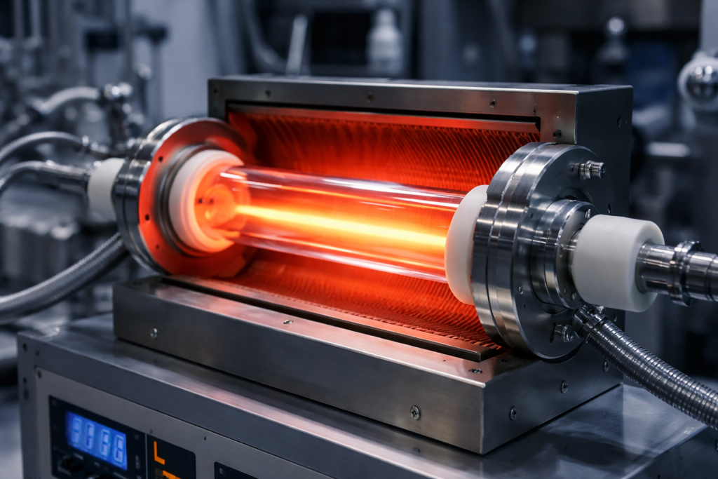
High-purity quartz is one of the most widely used materials inside semiconductor process equipment.
Quartz furnace tubes, wafer boats, injectors, liners, rings, flanges, process chambers and other custom components can be found in equipment used for:
- oxidation;
- diffusion;
- LPCVD;
- CVD;
- ALD;
- annealing;
- epitaxy;
- plasma etching;
- wafer cleaning;
- thermal processing.
The reason is straightforward.
Fused quartz combines:
- high-temperature capability;
- very low thermal expansion;
- excellent thermal-shock resistance;
- high chemical resistance;
- electrical insulation;
- relatively low contamination;
- good dimensional stability.
However, the phrase “high-purity quartz” is often misunderstood.
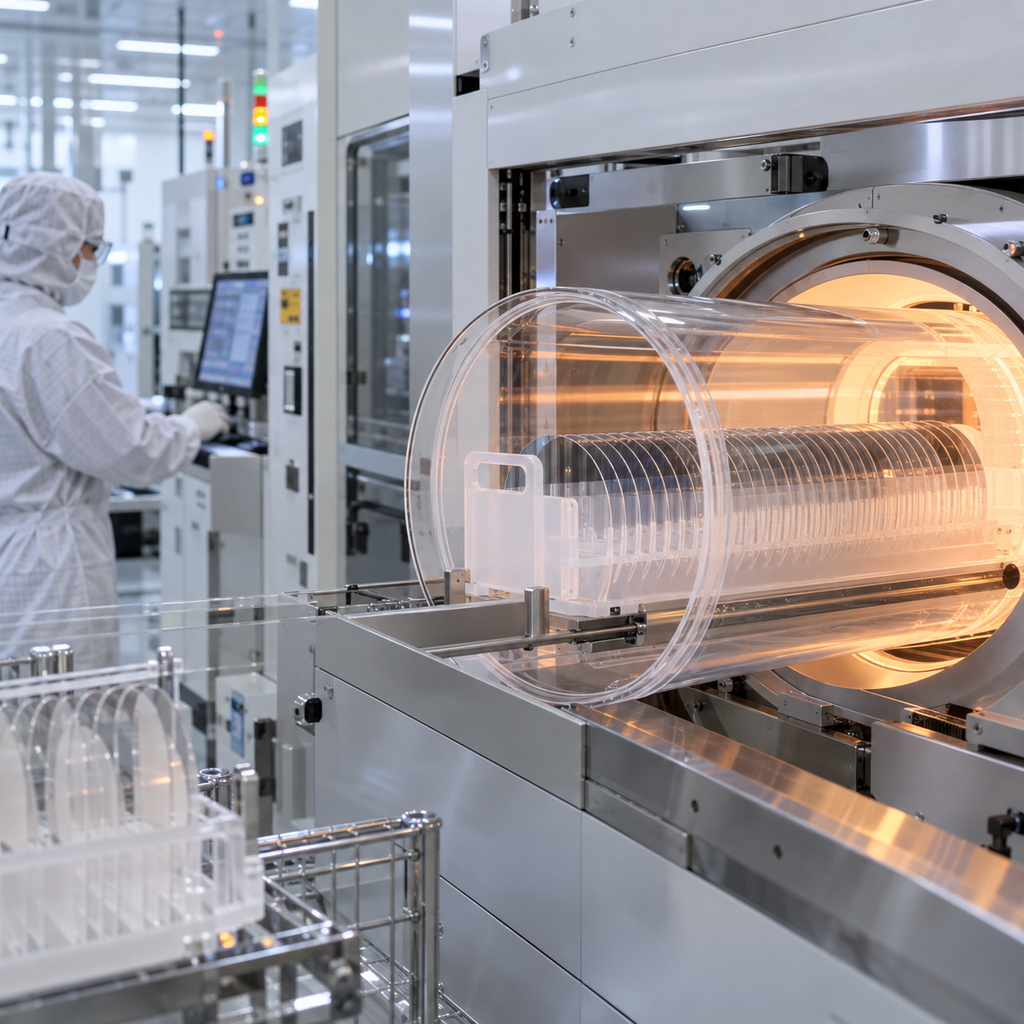
A semiconductor purchaser should not evaluate a quartz component only by asking:
Is the material 99.99% or 99.999% SiO₂?
For advanced semiconductor applications, especially DRAM, NAND and 300 mm wafer processing, individual trace impurities can be more important than the headline SiO₂ percentage.
Key parameters can include:
Li → Na → K → Al → Fe → Ca → Cu → Cr → Ni → OH → bubbles → inclusions → particles → devitrification → dimensional stability → cleaning history
The finished component must also pass customer-specific qualification.
This guide explains how to evaluate high-purity quartz for semiconductor equipment and what should be included in a quartz component RFQ.
1. Why Quartz Is Used in Semiconductor Equipment
Semiconductor processing often exposes equipment components to extreme environments.
These may include:
- temperatures above 1000°C in furnace processes;
- aggressive process gases;
- repeated heating and cooling;
- plasma environments;
- high-purity chemical cleaning;
- tight particle limits;
- long process cycles.
Conventional glass cannot tolerate many of these conditions.
Fused quartz has an amorphous SiO₂ structure and an exceptionally low coefficient of thermal expansion, which gives it strong resistance to rapid temperature changes.
For batch processing, quartz components are commonly used in vertical and horizontal furnaces containing large numbers of wafers. Heraeus notes that batch CVD-related processes can handle roughly 100–160 or more wafers in one furnace run, making chamber cleanliness and material stability particularly important because one component can potentially affect many wafers simultaneously.
Typical quartz semiconductor components include:
Quartz Furnace Tubes
Used as process chambers in diffusion, oxidation, annealing and deposition furnaces.
Quartz Wafer Boats
Hold multiple wafers at controlled pitch during batch thermal processes.
Quartz Injectors
Introduce process gases into the reaction zone.
Quartz Liners
Protect process chambers and control gas or thermal environments.
Quartz Rings
Used in etching, deposition and wafer-support assemblies.
Quartz Flanges
Connect quartz chambers with process equipment and sealing systems.
Quartz Plates and Windows
Used for process isolation, optical access, plasma systems and equipment structures.
2. What Does “High-Purity Quartz” Actually Mean?
Quartz purity is often expressed as the percentage of SiO₂.
Examples include:
4N = 99.99%
4N5 = 99.995%
5N = 99.999%
But this notation tells only part of the story.
Consider two hypothetical materials.
Material A
SiO₂: 99.999%
Na: relatively high
Material B
SiO₂: 99.995%
Na: much lower
For a semiconductor process sensitive to mobile alkali contamination, Material B could potentially be more appropriate even though its headline SiO₂ purity appears lower.
Therefore, semiconductor quartz should be evaluated using a trace-element profile, not purity percentage alone.
Commercial semiconductor quartz specifications illustrate this clearly. For example, Heraeus publishes individual concentrations for Li, Na, K, Fe, Cu, Cr, Ni, Ti, Zr, Al and other elements instead of relying on one total-purity figure.
3. Why Alkali Metals Matter
Among the most important contaminants are:
- lithium — Li;
- sodium — Na;
- potassium — K.
These elements are collectively referred to as alkali metals.
Their concentrations can be very small, often expressed in parts per million or even lower, yet they are still important in semiconductor manufacturing.
Mobile-Ion Contamination
Alkali ions—especially sodium—can be highly mobile under electrical fields and elevated temperatures.
In semiconductor structures, unwanted ionic contamination can affect:
- dielectric reliability;
- threshold-voltage stability;
- gate oxide behavior;
- surface charge;
- device lifetime.
Therefore, minimizing sodium and potassium is particularly important for semiconductor-contact materials.
Alkali Metals and Quartz Stability
There is another reason alkalis matter.
They can promote devitrification of quartz glass.
Heraeus describes sodium and potassium as among the most common contaminants that promote devitrification by disrupting the silica network and acting as nucleation sources at elevated temperature.
This means alkali contamination can create two risks simultaneously:
wafer contamination + shortened quartz-component lifetime
4. Typical Trace-Metal Levels in Semiconductor Quartz
There is no single impurity specification that defines every semiconductor application.
Different processes use different quartz grades.
However, commercial data show how large the differences can be.
For example, Heraeus lists typical electrically fused semiconductor quartz with approximately:
- Li: ~0.5 ppm
- Na: ~0.1–0.2 ppm
- K: ~0.2–0.3 ppm
- Fe: ~0.1 ppm
- Al: ~15 ppm
depending on material grade.
By comparison, some synthetic fused-silica grades are specified with many metallic impurities below 0.01 ppm, with certain elements even lower.
Another synthetic semiconductor material, Spectrosil 1000, is reported with the sum of selected metallic impurities at approximately 50 ppb, illustrating how far contamination levels can be reduced when synthetic material is required.
These numbers should be viewed as examples of commercially available material—not universal acceptance limits.
The correct requirement depends on:
- process node;
- device type;
- process chemistry;
- chamber location;
- wafer proximity;
- process temperature;
- customer contamination budget.
5. Aluminum Is Different from Sodium
Aluminum deserves separate attention.
Natural-quartz-derived fused material can contain considerably more Al than Na or K.
For example, some commercial natural semiconductor quartz grades list aluminum in the range of several to around 15 ppm while maintaining alkali metals at fractions of one ppm.
This does not automatically mean the material is unsuitable.
Aluminum behaves differently from mobile alkali ions.
The acceptable level depends on the process.
For increasingly demanding applications, manufacturers may therefore offer special low-Al quartz grades.
Heraeus, for example, describes TSC-4 as a semiconductor material designed with reduced Al and alkali-metal concentrations for demanding applications.
Therefore an RFQ stating:
Total purity ≥99.999%
may be less useful than specifying:
Na ≤ ___ ppm
K ≤ ___ ppm
Li ≤ ___ ppm
Al ≤ ___ ppm
Fe ≤ ___ ppm
when particular contamination species matter.
6. Why Iron and Transition Metals Matter
Transition-metal contaminants can also be critical.
Typical monitored elements include:
- Fe;
- Cu;
- Ni;
- Cr;
- Mn.
These materials can potentially affect semiconductor devices through contamination, diffusion or defect-generation mechanisms.
For high-purity quartz, the impurity certificate should therefore include more than only alkali metals.
A useful trace-metal certificate may include:
| Element | RFQ Requirement |
|---|---|
| Li | ___ ppm |
| Na | ___ ppm |
| K | ___ ppm |
| Mg | ___ ppm |
| Ca | ___ ppm |
| Fe | ___ ppm |
| Cu | ___ ppm |
| Cr | ___ ppm |
| Ni | ___ ppm |
| Mn | ___ ppm |
| Ti | ___ ppm |
| Al | ___ ppm |
The exact limits should be determined according to the customer’s process.
7. What Is OH Content?
OH refers to hydroxyl groups incorporated into the quartz-glass network.
OH content is normally expressed in:
ppm by weight
The manufacturing process strongly affects OH concentration.
Some electrically fused quartz grades can have OH below approximately 30 ppm, while certain synthetic fused-silica grades may contain approximately 150–200 ppm or much more. Conversely, specialized synthetic material can also be produced with very low OH.
Therefore:
synthetic quartz does not automatically mean low OH.
And:
low OH does not automatically mean highest purity in every other parameter.
These properties must be evaluated separately.
8. Why OH Matters in Semiconductor Quartz
OH can influence several properties.
High-Temperature Behavior
Hydroxyl content can influence viscosity and structural behavior at high temperatures.
For furnace components that must remain mechanically stable during extended thermal cycles, OH level may therefore be part of material selection.
Optical Absorption
OH creates characteristic absorption in the infrared.
This is especially important for optical quartz but can also matter when semiconductor equipment uses infrared heating or monitoring.
Process Compatibility
Some processes may favor low-OH electrically fused material, while others may benefit from extremely high chemical purity offered by synthetic fused silica even if the OH level is higher.
Therefore, asking only:
Is low OH better?
is not the right question.
The better question is:
What combination of OH, trace metals and high-temperature stability is required for this process?
9. High Purity vs Low OH: They Are Not the Same Specification
This is an important procurement concept.
Consider two general material types.
Electrically Fused Natural Quartz
Potential advantages:
- low OH;
- good high-temperature behavior;
- established semiconductor usage;
- favorable cost for many furnace components.
Potential limitation:
- natural quartz raw material introduces higher levels of certain trace elements such as Al.
Synthetic Fused Silica
Potential advantages:
- extremely low metallic contamination;
- excellent batch consistency;
- very low inclusions in premium grades.
Potential limitation:
- some synthetic production routes produce relatively high OH.
Commercial Heraeus data demonstrate this clearly: certain electrically fused grades list OH below 30 ppm, while a synthetic HSQ-T material lists OH around 150–200 ppm but extremely low trace metals.
Therefore material selection is a trade-off, not a one-dimensional purity ranking.
10. What Is Devitrification?
Fused quartz is amorphous.
Its SiO₂ molecules do not form the ordered lattice found in crystalline quartz.
At elevated temperature, however, fused quartz can gradually transform into crystalline forms of silica.
This phenomenon is called:
devitrification
Devitrified areas may appear:
- white;
- cloudy;
- rough;
- opaque.
Devitrification is undesirable because it can change:
- surface condition;
- dimensional stability;
- mechanical strength;
- particle performance;
- thermal behavior.
Heraeus explains that quartz glass is thermodynamically driven toward a crystalline state, but its high viscosity normally prevents rapid structural rearrangement. Elevated temperature and contamination can accelerate nucleation and crystallization.
11. Why Sodium and Potassium Accelerate Devitrification
Clean high-purity quartz can remain stable for long periods under appropriate operating conditions.
Surface contamination changes this behavior.
Alkali metals such as:
- Na;
- K
can disrupt the silica network and provide nucleation sites for crystallization.
Therefore one of the most important lessons for semiconductor quartz is:
High-purity raw material can still devitrify rapidly if the finished component becomes contaminated during machining, handling or cleaning.
This means material purity alone does not guarantee component lifetime.
The complete production chain matters.
12. Contamination Can Be Added During Fabrication
A high-purity quartz blank may leave the raw-material supplier with excellent chemical purity.
But subsequent manufacturing involves:
- cutting;
- grinding;
- CNC machining;
- flame welding;
- polishing;
- ultrasonic cleaning;
- manual handling;
- packaging.
Every step can introduce contamination.
Possible contamination sources include:
- grinding tools;
- coolant;
- polishing slurry;
- metal fixtures;
- dirty gloves;
- shop dust;
- cleaning chemicals;
- packaging material.
For this reason, semiconductor quartz manufacturing requires contamination control throughout the process—not simply the purchase of high-purity raw material.
13. Surface Purity Can Matter More Than Bulk Purity
Bulk ICP analysis tells the customer what is inside the quartz material.
It does not automatically tell the customer what is present on the finished surface.
For semiconductor process components, surface contamination can be especially important because the wafer and process gas interact with the component surface.
For critical applications, qualification may therefore evaluate both:
bulk trace elements
and
surface cleanliness
Possible analytical methods include:
- ICP-MS;
- ICP-OES;
- ion chromatography;
- surface extraction;
- particle inspection.
The actual test method should be agreed with the customer.
14. Particles Are a Different Contamination Problem
A quartz component can meet chemical purity requirements and still fail because of particles.
Particle sources may include:
- rough machined surfaces;
- damaged edges;
- microcracks;
- devitrified regions;
- residual polishing compound;
- contaminated packaging;
- plasma erosion.
This is particularly important in:
- advanced DRAM;
- NAND;
- ALD;
- plasma etching;
- high-aspect-ratio processing.
A single particle can potentially create a wafer defect.
Therefore qualification should include surface condition and cleanliness, not just chemistry.
15. Why DRAM and NAND Put Greater Pressure on Quartz Components
Modern memory structures rely increasingly on complex three-dimensional architectures.
In advanced DRAM and NAND manufacturing, equipment must perform highly controlled:
- deposition;
- etching;
- annealing;
- cleaning.
Heraeus specifically notes that continued 3D integration in DRAM and NAND increases the need for plasma etching of high-aspect-ratio structures, while deposition requires increasingly uniform films over complex 3D features.
As structures become more difficult to manufacture, the contamination budget becomes increasingly restrictive.
Quartz components that previously performed adequately in a mature process may therefore require:
- lower trace metals;
- improved particle performance;
- more consistent cleaning;
- tighter dimensions;
- improved plasma resistance.
16. High-Purity Quartz for LPCVD and Furnace Processing
LPCVD and thermal furnaces commonly use:
- furnace tubes;
- wafer boats;
- injectors;
- paddles;
- liners.
Important material requirements include:
Chemical Purity
Quartz should not introduce unwanted impurities into the furnace environment.
High-Temperature Stability
Long process times can cause deformation or sagging if material selection is inappropriate.
Devitrification Resistance
Surface contamination must be minimized.
Geometry
Tube straightness, roundness and dimensional tolerances affect equipment assembly and gas flow.
Thermal Cycling
Components must tolerate repeated heating and cooling without cracking.
Commercial quartz suppliers therefore offer different furnace-material grades optimized for standard and high-temperature environments rather than using one generic quartz composition for every tube.
17. Quartz for ALD and PEALD
Atomic layer deposition requires extremely controlled film growth.
In ALD:
one process cycle may deposit only a fraction of a nanometer to a few angstrom-level increments, depending on chemistry.
This makes contamination and chamber-condition stability highly important.
High-purity quartz may be used in:
- chamber liners;
- process tubes;
- injectors;
- support parts.
Heraeus places selected and synthetic quartz grades into increasingly demanding CVD, ALD and PEALD applications, reflecting the movement toward tighter contamination control.
For highly sensitive deposition applications, synthetic quartz with extremely low metal contamination may therefore justify its higher material cost.
18. Quartz Components for Plasma Etching
Quartz and fused silica are also used in plasma etch equipment.
Typical components can include:
- rings;
- windows;
- plates;
- liners;
- process shields.
The challenge differs from furnace processing.
Here, the material may be exposed to:
- energetic plasma;
- fluorine-containing chemistry;
- ion bombardment;
- thermal cycling.
Material erosion can eventually contribute to:
- particles;
- dimensional change;
- contamination.
Synthetic fused silica is available specifically for highly sensitive plasma etch and deposition systems. Heraeus reports ultra-low-metal synthetic material designed to reduce contamination risk in plasma etch and ALD applications.
19. Natural Quartz vs Synthetic Quartz for Semiconductor Equipment
A simplified comparison is useful.
| Parameter | Natural-Quartz-Derived Fused Quartz | Synthetic Fused Silica |
|---|---|---|
| Raw material | High-purity natural quartz | Chemically synthesized precursor |
| Cost | Generally lower | Generally higher |
| Alkali metals | Low in semiconductor grades | Can be extremely low |
| Aluminum | Usually higher | Can be extremely low |
| OH | Can be very low | Process-dependent, often higher |
| High-temperature furnace use | Widely used | Application dependent |
| Ultra-sensitive etch/ALD | Possible by grade | Often preferred for highest purity |
| Semiconductor use | Extensive | Extensive in demanding applications |
This is not a universal ranking.
The appropriate material depends on where the component sits inside the tool.
20. Do All Quartz Parts Need Synthetic Material?
No.
Specifying synthetic fused silica for every semiconductor component can substantially increase cost without improving process performance.
A better strategy is to classify parts according to contamination sensitivity.
For example:
Lower Sensitivity
External support or non-critical structures.
Medium Sensitivity
Conventional furnace and CVD components.
High Sensitivity
Components close to the wafer or process reaction zone.
Ultra-High Sensitivity
Advanced ALD, plasma etch, highly contamination-sensitive processes.
Material grade should then be selected accordingly.
This creates a better balance between:
purity + performance + component lifetime + cost
21. Quartz Component Qualification Is More Than Material Certification
A raw-material certificate is only the beginning.
A DRAM fab or semiconductor equipment manufacturer generally needs confidence in the finished component and manufacturing process.
A qualification program may include several stages.
Stage 1 — Raw Material Review
Review:
- raw-material source;
- material grade;
- trace-metal analysis;
- OH content;
- bubble/inclusion specification;
- lot identification.
Stage 2 — Dimensional Qualification
Inspect:
- OD;
- ID;
- wall thickness;
- flatness;
- straightness;
- slot pitch;
- flange dimensions;
- concentricity.
Stage 3 — Visual Inspection
Inspect for:
- cracks;
- chips;
- scratches;
- bubbles;
- inclusions;
- weld defects;
- polishing defects.
Stage 4 — Cleanliness Qualification
Review:
- cleaning procedure;
- final rinse;
- particle control;
- ionic contamination;
- packaging environment.
Stage 5 — Thermal Qualification
Where applicable, evaluate:
- repeated thermal cycling;
- distortion;
- sagging;
- devitrification;
- weld stability.
Stage 6 — Tool Qualification
Install components into actual or representative equipment and evaluate:
- particles;
- chamber performance;
- process repeatability;
- wafer contamination;
- film uniformity;
- defect level.
Stage 7 — Production Qualification
Only after stable process performance is demonstrated should a part or material move into routine production supply.
Exact procedures are customer-specific.
There is no single universal “DRAM quartz qualification standard.”
22. Why Lot-to-Lot Consistency Matters
A supplier can produce one excellent sample and still fail as a semiconductor supplier.
High-volume fabs require repeatability.
Important parameters include:
- raw material source;
- impurity distribution;
- tube dimensions;
- welding process;
- surface finish;
- cleaning;
- packaging.
A mature qualification therefore evaluates not only initial samples but also multiple production lots.
For high-volume DRAM production, consistency can be more important than achieving an exceptional result on one prototype.
23. Change Control Is Part of Qualification
Once a component is qualified, major manufacturing changes cannot necessarily be introduced without customer review.
Examples include:
- changing quartz raw-material grade;
- changing raw-material supplier;
- modifying welding parameters;
- changing polishing compound;
- changing cleaning chemistry;
- changing final packaging;
- moving production to another manufacturing line.
These changes may affect contamination or component performance.
Therefore semiconductor customers may require:
PCN — Process Change Notification
or an equivalent change-control procedure.
For serious semiconductor supply, traceability and change control should be built into the supplier’s quality system.
24. What Documents Should a Quartz Supplier Provide?
Depending on the customer, useful documents may include:
Certificate of Conformance
Confirms the component meets the agreed drawing and specification.
Material Certificate
Identifies the quartz grade and batch.
Chemical Purity Data
Provides trace-element concentrations.
Dimensional Inspection Report
Reports critical dimensions.
Visual Inspection Record
Documents chips, scratches, cracks and weld condition.
Cleaning Record
Confirms the required cleaning process.
Packaging Specification
Describes clean packaging method.
Lot Traceability
Allows the component to be linked back to raw material and manufacturing history.
For higher-level qualification, customers may request additional analytical reports.
25. Recent DRAM Qualification Shows Why Validation Matters
High-purity quartz has recently attracted greater attention as semiconductor supply chains diversify.
In September 2026, reports stated that high-purity quartz products from Jiangsu Pacific Quartz had passed qualification at a Chinese DRAM manufacturer for components used in 300 mm wafer production. Reports also noted previous supply relationships with major semiconductor equipment makers for products such as LPCVD tubes and quartz boats. The identity of the DRAM customer has been attributed by industry analysts to CXMT, but that identification was not presented as an official customer confirmation in the reporting.
The important engineering point is not the company name.
It is the qualification process itself.
Semiconductor quartz does not enter a DRAM production line simply because a supplier can manufacture 5N material.
The material, finished component, cleaning process, consistency and actual tool performance must all be validated.
This is a critical distinction between:
high-purity quartz material
and
qualified semiconductor quartz components.
26. Quartz for Semiconductor Equipment vs Quartz Crucibles
Another common misunderstanding is treating all semiconductor quartz as one market.
There are two very different applications.
Semiconductor Process Equipment
Examples:
- furnace tubes;
- wafer boats;
- injectors;
- quartz rings;
- plates;
- liners.
These components are used after a silicon wafer has already been produced.
Silicon Crystal-Growth Crucibles
Quartz crucibles are used during the Czochralski process to grow silicon ingots.
These crucibles have different requirements because contamination can directly enter the silicon melt.
Recent industry reporting has highlighted this distinction: progress in qualifying high-purity quartz for semiconductor equipment does not automatically mean the same supplier can meet the more demanding raw-material requirements for advanced silicon crystal-growth crucibles.
Therefore:
LPCVD tube quartz ≠ CZ crucible quartz
even though both may be described as high-purity quartz.
27. Common Quartz Qualification Failure Modes
A component can fail semiconductor qualification for many reasons.
Trace Metal Too High
Na, K, Li, Al, Fe or other elements exceed the agreed limit.
Surface Contamination
Bulk material passes, but fabrication introduces metals or particles.
Excessive Particles
Cleaning or surface finishing is inadequate.
Devitrification
Quartz becomes cloudy or crystalline after high-temperature exposure.
Distortion
Tube, boat or flange geometry changes after thermal cycling.
Slot Error
Wafer boat pitch or slot dimensions fail requirements.
Weld Failure
Thermal stress exposes weaknesses in welded joints.
Chipping
Edges generate particles during handling.
Packaging Contamination
A clean component becomes contaminated after final inspection.
Successful qualification therefore requires control from raw material through final packaging.
28. Incoming Inspection for Semiconductor Quartz Components
A semiconductor customer receiving new quartz parts should consider checking:
- Part number and drawing revision
- Raw material grade
- Lot number
- Dimensions
- Chips and cracks
- Surface condition
- Weld quality
- Cleanliness
- Packaging integrity
- Certification documents
For critical processes, periodic verification of trace metals or particles may also be appropriate.
This helps prevent an apparently identical replacement part from introducing a process change.
29. How to Write an RFQ for High-Purity Quartz Components
A useful RFQ should include more than:
Need semiconductor quartz tube, 99.999% purity.
Instead provide:
Part Information
- Quartz tube / boat / ring / plate / flange / injector
- Drawing
- Part number
- Revision
Dimensions
- OD
- ID
- Length
- Wall thickness
- Tolerances
Material Requirement
- Natural fused quartz / synthetic fused silica
- Required material grade if known
- Minimum SiO₂ purity if required
Trace Elements
Specify limits where necessary for:
- Li
- Na
- K
- Al
- Fe
- Ca
- Cu
- Cr
- Ni
OH
- Maximum or target OH if required
Process
- LPCVD
- oxidation
- diffusion
- ALD
- PEALD
- annealing
- plasma etch
- epitaxy
Temperature
- maximum operating temperature
- process duration
- heating/cooling cycle
Cleaning
- semiconductor cleaning requirement
- particle specification
- final rinse requirements
Documentation
- material certificate
- trace-metal report
- dimensional report
- CoC
Quantity
- prototype
- qualification lot
- production quantity
Providing this information allows the supplier to recommend the appropriate quartz grade instead of automatically selecting the most expensive material.
30. Example RFQ — LPCVD Quartz Tube
Product: High-Purity Quartz Furnace Tube
Application: LPCVD
Wafer Size: 300 mm
Material: Semiconductor-grade fused quartz
OD: ___ mm
ID: ___ mm
Length: ___ mm
Wall Thickness: ___ mm
Maximum Temperature: ___ °C
Na: ≤ ___ ppm
K: ≤ ___ ppm
Li: ≤ ___ ppm
Al: ≤ ___ ppm
OH: ≤ ___ ppm if required
Surface: Semiconductor-clean
Documentation: Material Certificate + Dimensional Report + CoC
Quantity: 3 qualification pcs + production forecast
31. Example RFQ — Quartz Wafer Boat
Product: High-Purity Quartz Wafer Boat
Application: DRAM Furnace / CVD
Wafer Diameter: 300 mm
Wafer Capacity: ___ pcs
Slot Pitch: ___ mm
Slot Width: ___ mm
Material Grade: ___
Maximum Operating Temperature: ___ °C
Particle Requirement: Customer specified
Cleaning: Semiconductor grade
Quantity: ___ pcs
For wafer boats, dimensional consistency is particularly important because pitch and slot geometry directly affect wafer handling.
32. Example RFQ — Plasma Etch Quartz Ring
Product: Quartz Process Ring
Application: Plasma Etch
Wafer Diameter: 300 mm
Material: High-purity natural quartz / synthetic fused silica
OD: ___ mm
ID: ___ mm
Thickness: ___ mm
Flatness: ___
Surface Roughness: ___
Trace Metals: Customer specification
Particle Requirement: Customer specification
Quantity: Qualification + production volume
For plasma applications, material selection should also consider expected erosion and component replacement cycle.
33. Supplier Evaluation Checklist
When evaluating a high-purity quartz component supplier, ask:
Raw Material
Can the supplier identify the original quartz material and lot?
Trace Metal Control
Can impurity information be provided?
Semiconductor Cleaning
Does the supplier use a defined final cleaning process?
Machining Capability
Can critical geometry and tolerance be controlled?
Welding
Can welded tubes, flanges and injectors survive thermal cycles?
Inspection
Are critical dimensions and surface defects inspected?
Packaging
Is the final component protected from recontamination?
Traceability
Can finished parts be traced to production and material lots?
Qualification Support
Can prototypes and qualification lots be supplied before mass production?
These questions are usually more valuable than asking only:
What is your quartz purity?
Conclusion
High-purity quartz is essential for semiconductor manufacturing, but purity should never be reduced to a single SiO₂ percentage.
For DRAM, NAND and advanced semiconductor equipment, the real material-performance relationship is:
raw-material purity
→ alkali metals
→ transition metals
→ aluminum
→ OH content
→ bubbles and inclusions
→ fabrication contamination
→ surface particles
→ devitrification
→ thermal stability
→ dimensional control
→ cleaning
→ qualification
Na and K are particularly important because they can contribute both to semiconductor contamination and to quartz devitrification.
OH must be considered separately from metallic purity: low-OH electrically fused quartz and ultra-high-purity synthetic fused silica can serve different process requirements.
Most importantly, high-purity material is not the same as a qualified semiconductor component.
For a quartz tube, wafer boat, injector, ring or flange to enter a DRAM or other semiconductor production environment, the supplier must demonstrate repeatable control of the complete manufacturing process.
Fuyao Quartz can manufacture custom high-purity quartz components for semiconductor-equipment applications, including:
- quartz furnace tubes;
- quartz wafer boats;
- quartz injectors;
- quartz flanges;
- quartz rings;
- quartz plates;
- quartz liners;
- custom welded quartz assemblies.
Customers can provide the drawing, quartz grade, operating temperature, wafer size, trace-metal requirements, OH requirement, cleaning specification and qualification quantity for technical evaluation and quotation.
FAQ
Is 99.999% quartz automatically semiconductor grade?
No. Total SiO₂ purity does not completely define semiconductor suitability. Individual Na, K, Li, Al, Fe and other impurities, as well as particles, cleaning and component processing, must also be considered.
Why are sodium and potassium important in semiconductor quartz?
They are undesirable mobile ionic contaminants and can also accelerate devitrification of fused quartz at elevated temperatures.
Is lower OH always better?
No. OH content and metallic purity are separate properties. Some ultra-high-purity synthetic fused silica has higher OH than electrically fused natural quartz. The correct material depends on the actual semiconductor process.
What causes quartz devitrification?
High temperature allows fused quartz to move toward a crystalline state. Surface contamination—especially alkali contamination such as sodium or potassium—can accelerate nucleation and crystallization.
What is the difference between semiconductor quartz tubes and quartz crucibles?
Process tubes are used inside semiconductor manufacturing equipment after wafers have been produced. Quartz crucibles are used earlier to grow silicon ingots and have a different contamination environment and material specification.
Does DRAM manufacturing require synthetic quartz for every component?
No. Material selection depends on component location, temperature, process chemistry and contamination sensitivity. Semiconductor-grade natural fused quartz remains widely used, while synthetic material can be selected for especially contamination-sensitive processes such as advanced etch or deposition.
What information is needed for a semiconductor quartz RFQ?
Provide the drawing, component type, dimensions, wafer size, process type, maximum temperature, required material grade, impurity limits, OH requirements, cleaning requirements, documentation and qualification quantity.