Quartz wafers are increasingly used in semiconductor processing, MEMS fabrication, microfluidics, optical devices, sensor packaging, wafer-level bonding, and advanced research applications.
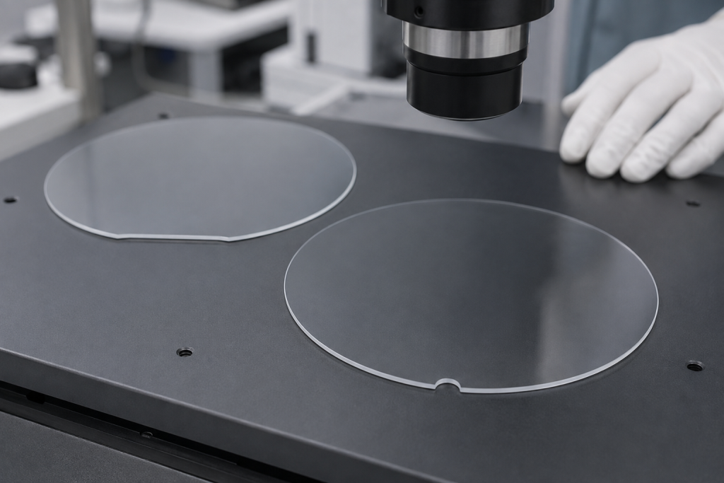
Although many quartz wafers are supplied as simple circular substrates, automated equipment often requires a notch or flat to identify the wafer’s rotational position. These features may look simple, but incorrect dimensions, ambiguous orientation definitions, or poor edge finishing can cause alignment errors, handling failures, edge chipping, and loss of usable process area.
This guide explains how to specify notch and flat features on fused quartz wafers, including orientation conventions, dimensional tolerances, edge-exclusion zones, inspection methods, and RFQ requirements.
Fused Quartz Wafers and Crystalline Quartz Wafers Are Different
This article mainly discusses wafers made from fused quartz or fused silica.
Fused quartz is an amorphous glass material. It does not have the crystallographic orientation found in silicon, sapphire, or single-crystal quartz.
Therefore, on a fused quartz wafer:
- A notch does not naturally indicate a crystal plane.
- A flat does not inherently identify a crystal direction.
- The feature usually serves as a mechanical or process reference.
- Its orientation must be defined by the customer’s drawing or fabrication process.
This is different from semiconductor-grade silicon wafers, where notches and flats may be associated with established crystallographic orientation and conductivity conventions.
Single-crystal quartz wafers are also different from fused quartz wafers. If the application requires a specific crystal cut, such as AT-cut or ST-cut quartz, crystallographic orientation must be defined separately.
The purchase specification should therefore clearly identify the material as:
- Fused quartz.
- Fused silica.
- Synthetic fused silica.
- Natural fused quartz.
- Single-crystal quartz.
Using only the term “quartz wafer” can create unnecessary ambiguity.
Why Quartz Wafers Need a Notch or Flat
A notch or flat provides a repeatable angular reference around the wafer circumference.
Depending on the application, it can be used for:
- Automated wafer alignment.
- Robotic handling.
- Lithography orientation.
- Coating direction control.
- Pattern alignment.
- Dicing reference.
- Wafer bonding alignment.
- Front-side and backside identification.
- Process tracking.
- Inspection-coordinate definition.
- Orientation of holes, channels, or patterned features.
Without a mechanical reference, a perfectly circular transparent wafer may be difficult for equipment to orient consistently.
This becomes especially important when the wafer contains asymmetric structures such as:
- Through-holes.
- Microfluidic channels.
- Metallized areas.
- Optical apertures.
- Patterned coatings.
- Alignment marks.
- Local cavities.
- Bonding frames.
- Sensor arrays.
Notch vs. Flat: Which Should Be Used?
Both features can establish wafer orientation, but their geometry and equipment compatibility are different.
| Feature | Description | Main advantages | Main considerations |
|---|---|---|---|
| Notch | A small recess machined into the wafer circumference | Preserves most of the circular wafer area and is compatible with many alignment systems | Requires careful machining and a controlled root radius |
| Flat | A straight section machined along part of the circumference | Easy to identify visually and measure | Removes more usable wafer area and may affect handling geometry |
| No feature | Fully circular wafer | Maximum usable circular area | Requires optical marks, fixtures, or another alignment method |
A notch is generally preferred when preserving wafer area is important or when equipment is designed to detect a localized orientation feature.
A flat may be more practical for:
- Manual alignment.
- Laboratory fixtures.
- Legacy equipment.
- Custom optical assemblies.
- Small-volume research projects.
- Applications requiring a broad mechanical reference surface.
The final decision should be based on downstream equipment rather than appearance alone.
Quartz Wafer Notch Geometry
A complete notch specification requires more than stating “standard notch.”
The drawing should define:
- Notch shape.
- Notch opening width.
- Notch depth.
- Included angle, when applicable.
- Root radius.
- Edge blending.
- Position relative to the wafer center.
- Angular orientation tolerance.
- Surface and edge finish.
Notch Shape
Common notch configurations include:
- Rounded V-shaped notch.
- U-shaped notch.
- Semicircular notch.
- Customer-defined alignment recess.
For brittle quartz materials, a sharp internal corner should generally be avoided because it can concentrate mechanical stress.
A controlled root radius helps reduce the risk of:
- Microcrack formation.
- Edge chipping.
- Crack propagation.
- Breakage during cleaning.
- Failure during robotic handling.
- Damage during thermal cycling.
The notch geometry must also remain compatible with the optical or mechanical sensor used by the customer’s equipment.
Notch Width and Depth
Notch dimensions should be large enough for reliable detection but not so large that they unnecessarily reduce the usable area or weaken the wafer edge.
For custom fused quartz wafers, the appropriate notch size depends on:
- Wafer diameter.
- Wafer thickness.
- Equipment sensor resolution.
- Required alignment accuracy.
- Edge-exclusion requirements.
- Machining limitations.
- Acceptable mechanical strength.
A specification should show both the nominal notch width and nominal depth, together with individual tolerances.
Avoid relying only on a reference photograph. A dimensional drawing is required for repeatable production.
Quartz Wafer Flat Geometry
A wafer flat is normally specified by its chord length and location relative to the wafer center.
Important parameters include:
- Flat length.
- Distance from the wafer center to the flat.
- Angular orientation.
- Straightness.
- Edge finish.
- Transition radius at both ends.
- Relationship to other wafer features.
The ends of the flat should transition smoothly into the circular edge. Abrupt corners can become stress-concentration points and increase the risk of chipping.
A flat also changes the usable wafer outline more than a small notch. The device layout and edge-exclusion zone should therefore be checked before the flat length is finalized.
Defining Wafer Orientation Correctly
Orientation is one of the most common sources of drawing errors.
A supplier needs to know exactly how the notch or flat relates to every other feature on the wafer.
The drawing should define:
- Which surface is Side A.
- Which surface is Side B.
- Whether Side A is polished or coated.
- The viewing direction used for the drawing.
- The zero-degree reference direction.
- Whether angular measurements are clockwise or counterclockwise.
- The location of the notch or flat.
- The position of holes, channels, patterns, or coatings relative to the orientation feature.
Avoiding Mirrored Parts
A drawing can produce mirrored parts if it does not state whether the wafer is viewed from the front side or backside.
A good note would be similar to:
All feature locations are defined while viewing the polished Side A surface. Angular positions are measured clockwise from the notch centerline.
The wording can vary, but the viewing direction and angle convention must be unambiguous.
Does a Fused Quartz Notch Indicate Crystal Orientation?
No. Fused quartz and fused silica are amorphous materials.
The notch or flat is a customer-defined alignment reference unless the drawing states another purpose.
If the substrate is actually made from crystalline quartz, the required crystal cut and axis orientation must be specified independently.
Wafer Diameter and Thickness Specifications
Notch and flat dimensions should always be considered together with the main wafer geometry.
Common custom fused quartz wafer diameters include:
- 50.8 mm.
- 76.2 mm.
- 100 mm.
- 150 mm.
- 200 mm.
- 300 mm.
- Custom diameters.
The actual diameter should be stated numerically. Terms such as “4-inch wafer” or “8-inch wafer” may not define the exact nominal dimension and tolerance required by the equipment.
Relevant thickness specifications include:
- Nominal thickness.
- Thickness tolerance.
- Total thickness variation.
- Local thickness variation.
- Edge thickness.
- Minimum thickness near the notch or flat.
Typical quartz wafer thicknesses can range from thin research substrates to glass wafers measuring 1 mm or more. The correct thickness depends on handling, polishing, bonding, and process requirements.
Diameter and Notch Tolerance
The required tolerance depends on the application and manufacturing method.
Possible starting specifications for precision quartz wafers may include:
| Parameter | Example specification |
|---|---|
| Wafer diameter | 100.0 ± 0.1 mm |
| Wafer thickness | 500 ± 25 μm |
| Total thickness variation | ≤10 μm |
| Notch width | 2.0 ± 0.1 mm |
| Notch depth | 1.0 ± 0.1 mm |
| Notch orientation | ±1° |
| Edge-exclusion zone | 3 mm |
| Surface roughness | Defined by polished-side requirement |
These values are only an illustrative example, not a universal quartz wafer standard.
The final tolerance should reflect:
- Wafer diameter.
- Thickness.
- Equipment requirements.
- Machining method.
- Polishing method.
- Inspection capability.
- Required production volume.
Unnecessarily tight tolerances can increase cost without improving actual device performance.
Understanding Edge Exclusion
Edge exclusion is the peripheral area of a wafer that is not considered part of the guaranteed usable process region.
It may be excluded from requirements related to:
- Coating uniformity.
- Film thickness.
- Surface roughness.
- Flatness.
- Lithography.
- Particle inspection.
- Scratch-dig quality.
- Optical clear aperture.
- Device placement.
- Bonding performance.
Edge exclusion is normally measured radially inward from the wafer perimeter.
Common custom process definitions may use an edge exclusion of approximately:
1–5 mm
However, the correct value depends on the wafer diameter, edge profile, polishing process, coating equipment, and device layout.
Usable Diameter
For a circular wafer without a flat or notch, the approximate usable diameter can be described as:
Usable diameter = Wafer diameter − 2 × Edge exclusion
For example, a 100 mm wafer with a 3 mm edge exclusion has an approximate central usable diameter of 94 mm.
This simple calculation does not fully account for the local area around a notch or flat.
Local Keep-Out Area Around the Notch
A notch creates a localized interruption in the circular edge.
The process drawing should specify whether the normal edge-exclusion zone:
- Follows the notch contour.
- Is measured from the original nominal circle.
- Includes an additional local keep-out zone.
- Excludes a rectangular or radial area around the notch.
An additional keep-out zone may be required when:
- Devices are patterned close to the edge.
- A coating must remain uniform.
- Edge gripping equipment contacts the notch.
- Bonding seals are positioned near the perimeter.
- Automated inspection treats the notch as an irregular edge.
The same issue applies to wafer flats.
Edge Profile and Bevel Requirements
A wafer edge can be supplied in several conditions:
- As-cut.
- Ground.
- Chamfered.
- Rounded.
- Polished.
- Fire-finished.
- Customer-defined profile.
For precision wafer handling, a controlled rounded or beveled edge is generally preferable to a sharp square edge.
Benefits include:
- Reduced edge chipping.
- Improved handling reliability.
- Lower particle generation.
- Reduced crack initiation.
- Better compatibility with wafer carriers.
- More stable automated handling.
The edge profile should remain consistent around the notch or flat. A well-finished circular edge does not compensate for a poorly machined notch root.
Notch and Flat Manufacturing Process
A typical fused quartz wafer manufacturing sequence may include:
- Cutting the quartz blank.
- Grinding the outer diameter.
- Machining the notch or flat.
- Creating the specified edge profile.
- Lapping the wafer to the required thickness.
- Polishing one or both surfaces.
- Cleaning the wafer.
- Inspecting dimensions and surface quality.
- Packaging the wafer in a protective carrier.
The actual sequence may vary depending on wafer thickness, surface finish, and notch geometry.
For very thin wafers, machining the orientation feature requires careful process control because unsupported edges can chip or fracture.
Inspection of Notch and Flat Dimensions
Quartz wafer inspection should verify both the main wafer geometry and the localized orientation feature.
Wafer Diameter
Diameter can be measured using:
- Non-contact optical measurement.
- Coordinate measuring equipment.
- Precision vision systems.
- Calibrated mechanical instruments for less demanding tolerances.
For thin or high-precision wafers, non-contact methods help reduce the risk of edge damage.
Notch Width, Depth and Radius
An optical comparator or machine-vision system can be used to measure:
- Notch opening width.
- Maximum depth.
- Root radius.
- Included angle.
- Symmetry.
- Position relative to the wafer centerline.
The notch should also be inspected for small chips and microcracks that may not significantly change its measured dimensions.
Flat Length and Position
Flat inspection should verify:
- Chord length.
- Straightness.
- Distance from the center.
- Angular position.
- Transition geometry at both ends.
- Edge quality.
A flat with the correct length but incorrect rotational position may still make the wafer unusable.
Orientation Accuracy
Orientation is normally evaluated relative to:
- The wafer center.
- A defined datum.
- Patterned features.
- Holes or channels.
- Coating direction.
- Another alignment mark.
Angular tolerances should be shown directly on the drawing.
Edge and Notch Defect Inspection
The notch and flat areas are particularly vulnerable to mechanical damage.
Inspection should check for:
- Chips.
- Cracks.
- Microcracks.
- Grinding marks.
- Sharp internal corners.
- Inconsistent bevels.
- Local thinning.
- Surface contamination.
- Attached particles.
- Poorly blended transitions.
Useful inspection methods include:
- Bright-field microscopy.
- Dark-field illumination.
- Machine-vision inspection.
- Edge-profile measurement.
- Stress inspection using polarized light where appropriate.
- High-magnification inspection for critical parts.
Acceptance criteria should define the maximum permitted defect size and whether defects are allowed inside or outside the usable area.
TTV, Bow, Warp and Flatness
An orientation feature cannot compensate for poor overall wafer geometry.
A complete quartz wafer inspection may also include:
Total Thickness Variation
TTV is the difference between the maximum and minimum measured thickness across the wafer.
Excessive TTV can affect:
- Lithography focus.
- Bonding uniformity.
- Coating thickness.
- Chuck contact.
- Optical path length.
- Device alignment.
Bow
Bow describes the displacement of the wafer’s median surface relative to a reference plane when the wafer is in an unrestrained condition.
Warp
Warp represents the overall deviation of the wafer from a reference plane and can include more complex shape variation.
Bow and warp requirements should be defined according to the wafer diameter, thickness, polishing condition, and downstream equipment.
Surface and Optical Inspection
Depending on the application, quartz wafers may also require inspection for:
- Surface roughness.
- Scratches.
- Pits.
- Bubbles.
- Inclusions.
- Striae.
- Coating defects.
- Particles.
- Edge haze.
- Transmission uniformity.
- Clear-aperture quality.
For optical applications, specify:
- Wavelength range.
- Clear aperture.
- Surface quality.
- Surface flatness.
- Parallelism.
- Wedge.
- Coating requirements.
For semiconductor applications, particle control and cleaning may be more important than cosmetic appearance outside the usable area.
Common Notch and Flat Problems
Notch Chipping
Chipping can result from aggressive grinding, thin wafer edges, incorrect handling, or an excessively sharp notch geometry.
A larger controlled radius and improved edge finishing may reduce the risk.
Microcracks at the Notch Root
Microcracks can form even when the notch appears acceptable to the naked eye.
These cracks may grow during:
- Ultrasonic cleaning.
- Thermal cycling.
- Vacuum handling.
- Wafer bonding.
- Mechanical loading.
Microscopic inspection is recommended for critical applications.
Incorrect Angular Orientation
An incorrectly positioned notch can cause every patterned or fabricated feature on the wafer to be rotated relative to the equipment.
The inspection report should verify orientation, not only notch dimensions.
Notch Too Small for Equipment Detection
A small notch may preserve more usable area but may not be reliably recognized by an aligner or robotic handling system.
Equipment requirements should be confirmed before finalizing the drawing.
Flat Too Long
An unnecessarily long flat reduces usable substrate area and may interfere with edge gripping, bonding frames, or device placement.
Insufficient Local Edge Exclusion
Devices or coatings positioned too close to the notch can suffer from poor uniformity or mechanical damage.
A local keep-out zone should be included when necessary.
Inconsistent Edge Bevel
Changes in bevel geometry around the notch or flat can create weak points and increase particle generation.
Quartz Wafer RFQ Checklist
When requesting custom quartz wafers, provide the following information:
| Specification | Information required |
|---|---|
| Material | Fused quartz, fused silica, synthetic fused silica, or single-crystal quartz |
| Wafer diameter | Nominal diameter and tolerance |
| Thickness | Nominal thickness and tolerance |
| Surface finish | Single-side polished or double-side polished |
| Surface roughness | Required Ra and measurement method |
| TTV | Maximum acceptable value |
| Bow and warp | Maximum allowable values |
| Orientation feature | Notch, flat, or no orientation feature |
| Notch dimensions | Width, depth, radius, shape, and tolerance |
| Flat dimensions | Length, position, transition radius, and tolerance |
| Angular orientation | Datum, viewing direction, angle, and tolerance |
| Edge profile | Ground, chamfered, rounded, polished, or custom |
| Edge exclusion | Standard perimeter and local notch keep-out zone |
| Surface quality | Scratch-dig or defect requirements |
| Clear aperture | Required usable optical or processing area |
| Fabricated features | Holes, channels, cavities, coatings, or patterns |
| Cleaning | Standard cleaning or semiconductor-grade cleaning |
| Packaging | Individual packaging, cassette, or cleanroom packaging |
| Quantity | Prototype and production quantities |
| Application | MEMS, optics, bonding, coating, microfluidics, or research |
Example Drawing Specification
A practical custom wafer note might read:
Fused quartz wafer, diameter 100.0 ± 0.1 mm, thickness 500 ± 25 μm, double-side polished, TTV ≤10 μm. One rounded notch measuring 2.0 ± 0.1 mm wide and 1.0 ± 0.1 mm deep. Notch centerline orientation ±1°. All angular dimensions are defined while viewing polished Side A. Edge exclusion is 3 mm from the nominal circular edge, with an additional local keep-out zone around the notch. Notch and perimeter edges must be free from visible cracks and unacceptable chips.
The actual values should be adjusted according to the customer’s process and equipment.
Frequently Asked Questions
Does every fused quartz wafer need a notch?
No. A notch is only required when the process, equipment, inspection method, or device layout needs a repeatable angular reference. Fully circular quartz wafers are suitable for many optical and laboratory applications.
Does the notch indicate crystal orientation?
Not on fused quartz or fused silica wafers. These materials are amorphous. The notch is normally a customer-defined mechanical or process reference. Crystallographic orientation must be specified separately for single-crystal quartz.
How should edge exclusion be selected?
Edge exclusion should reflect the polishing process, edge profile, coating equipment, alignment method, device layout, and inspection requirements. A wider exclusion zone may be needed around a notch or flat.
Conclusion
A notch or flat is a small geometric feature with a major influence on wafer alignment, handling, inspection, and usable process area.
For fused quartz wafers, these features do not inherently represent crystal orientation. Their purpose and angular position must be defined through a clear drawing and an unambiguous viewing convention.
A complete quartz wafer specification should include the wafer diameter, thickness, TTV, bow, warp, notch or flat geometry, edge profile, orientation tolerance, edge exclusion, surface quality, cleaning, and packaging requirements.
Careful specification and inspection can reduce alignment errors, edge damage, particle generation, and compatibility problems in semiconductor, MEMS, optical, and microfluidic processes.
TAGS: Quartz Wafer, Fused Quartz Wafer, Fused Silica Wafer, Quartz Wafer Notch, Quartz Wafer Flat, Wafer Notch Size, Wafer Orientation, Wafer Edge Exclusion, Quartz Wafer Inspection, Quartz Wafer Dimensions, Quartz Wafer Tolerance, Wafer Edge Profile, Quartz Wafer TTV, Quartz Wafer Bow and Warp, Custom Quartz Wafer, Semiconductor Glass Wafer, Optical Quartz Substrate, Precision Quartz Fabrication