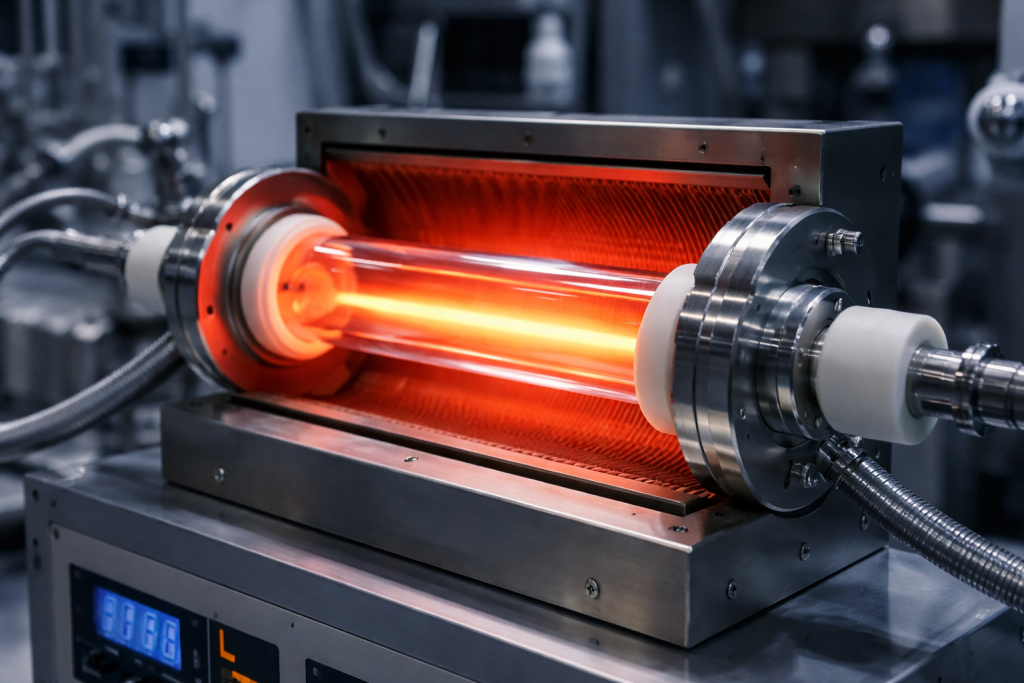
Anodic bonding is widely used to join borosilicate glass and silicon in microelectromechanical systems, pressure sensors, microfluidic devices, optical packages, and wafer-level assemblies. Among the available glass materials, BF33 borosilicate glass is frequently selected because of its thermal stability, optical transparency, chemical resistance, and relatively compatible thermal expansion with silicon.
However, successful bonding depends on more than choosing the correct glass. Bond temperature, applied voltage, surface cleanliness, wafer flatness, electrode configuration, and cooling conditions all influence bond strength and manufacturing yield.
This guide explains how BF33 anodic bonding works, which process parameters require attention, and how to identify common bonding defects before they become production problems.
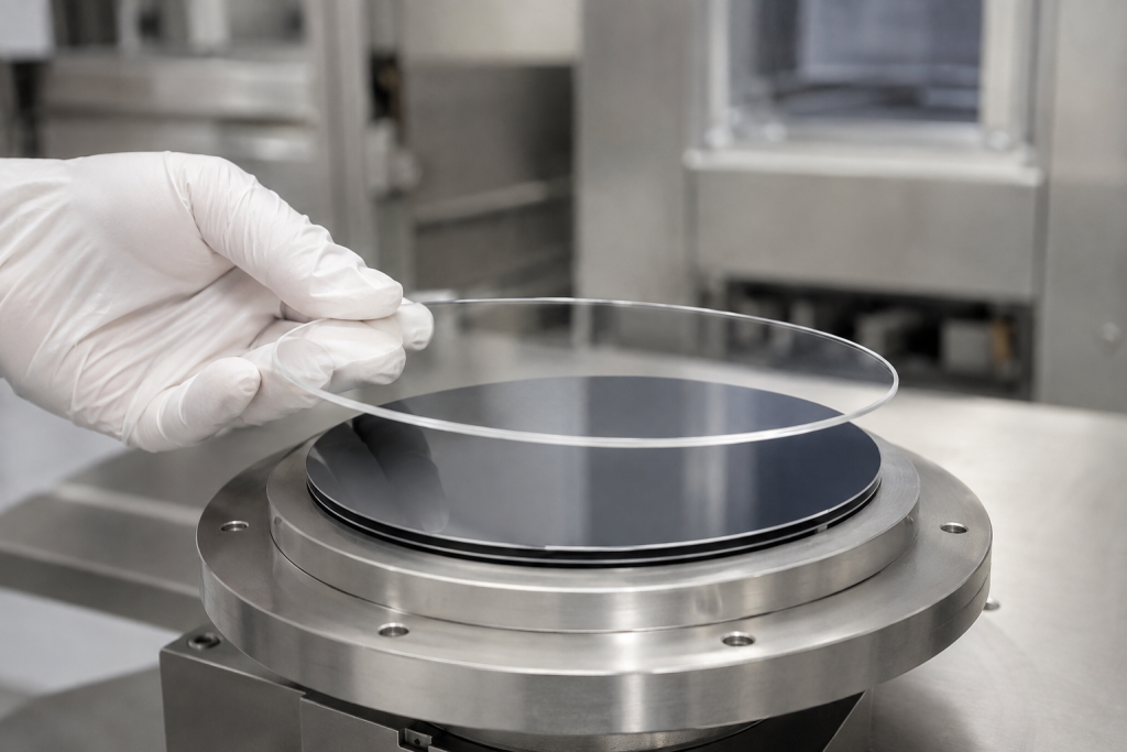
What Is BF33 Anodic Bonding?
Anodic bonding is a process that permanently joins an alkali-containing glass substrate to silicon using elevated temperature and an applied electric field.
During the process, the BF33 glass and silicon wafer are placed in close contact and heated. A voltage is applied across the assembly, typically with the silicon connected to the positive electrode and the outer glass surface facing the negative electrode.
At elevated temperatures, mobile alkali ions inside the glass migrate toward the negative electrode. Their movement creates an ion-depleted region near the glass-silicon interface. The resulting electric field pulls the two surfaces into intimate contact and promotes chemical bonding at the interface.
When the process is properly controlled, the bonded structure can provide:
- Strong adhesion between glass and silicon.
- Hermetic or near-hermetic sealing, depending on the design.
- Optical access through the glass substrate.
- Protection for sensitive silicon structures.
- Compatibility with wafer-level manufacturing.
- Stable performance in demanding operating environments.
The final result is not simply an adhesive connection. It is a direct glass-to-silicon bond formed through electrostatic attraction and interfacial chemical reactions.
Why BF33 Glass Is Used for Anodic Bonding
BF33 is a borosilicate glass material suitable for applications requiring a combination of optical transparency, dimensional stability, and chemical durability.
Its main advantages include:
Thermal Expansion Compatibility With Silicon
BF33 has a relatively low coefficient of thermal expansion compared with many conventional glass materials.
This helps reduce thermal stress when the bonded assembly cools from its bonding temperature to room temperature. Although the thermal expansion behavior of BF33 and silicon is not identical across the full temperature range, their compatibility is sufficient for many properly designed bonding applications.
Excessive differences in thermal expansion can otherwise contribute to:
- Wafer bow.
- Residual stress.
- Interface delamination.
- Glass cracking.
- Reduced long-term package reliability.
For larger wafers and thicker substrates, thermal stress management becomes especially important.
Optical Transparency
BF33 glass provides useful optical transparency for applications such as:
- Optical sensor packaging.
- Imaging devices.
- Microfluidic observation windows.
- MEMS inspection windows.
- Laboratory-on-chip systems.
- Photonic component protection.
When optical performance is critical, polishing quality, surface defects, thickness uniformity, and coating compatibility should be specified before production.
Chemical Resistance
Borosilicate glass offers good resistance to many chemicals used in laboratory and industrial environments.
This makes BF33 suitable for microfluidic devices and packaged components exposed to selected cleaning solutions, process fluids, or environmental contaminants.
However, chemical compatibility must still be evaluated for the actual operating media, especially when strong alkalis or hydrofluoric-acid-containing solutions are involved.
Availability in Wafer and Custom Substrate Formats
BF33 glass can be supplied as:
- Circular glass wafers.
- Square or rectangular substrates.
- Precision-cut windows.
- Drilled glass components.
- Custom microfluidic covers.
- Polished glass plates.
- Glass substrates with application-specific thicknesses.
The suitability of each format depends on the bonding equipment, silicon component geometry, and final packaging requirements.
Recommended BF33 Anodic Bonding Temperature
Bonding temperature controls the mobility of alkali ions inside the glass and strongly affects how quickly the interface forms.
Typical BF33 anodic bonding processes operate within approximately:
250°C to 450°C
For many standard glass-to-silicon applications, a practical starting development range is:
300°C to 400°C
The actual temperature should be established through process validation rather than selected from a general recommendation alone.
Lower Bonding Temperatures
Lower temperatures may be desirable when the assembly contains:
- Temperature-sensitive coatings.
- Metallized structures.
- Integrated electronic components.
- Polymer-compatible process interfaces.
- Preprocessed MEMS devices.
- Materials with limited thermal stability.
However, reducing the temperature can decrease ion mobility and slow bond formation. Compensation may require a different voltage profile, longer bonding time, improved surface activation, or specialized bonding equipment.
Higher Bonding Temperatures
Higher temperatures generally increase ion mobility and may help establish the bond more quickly.
However, excessive temperature can introduce problems such as:
- Increased thermal stress during cooling.
- Damage to temperature-sensitive structures.
- Oxidation or degradation of metallization.
- Increased wafer bow.
- Unwanted material reactions.
- Deformation of thin or fragile components.
For this reason, the best bonding temperature is usually the lowest validated temperature that consistently produces the required bond quality and throughput.
Applied Voltage and Electric Field
Anodic bonding requires an electric field across the glass-silicon assembly.
Typical development ranges are often approximately:
300 V to 1,200 V
Many production processes use settings within approximately:
400 V to 1,000 V
These values are not universal. The effective electric field depends on glass thickness, electrode design, material composition, temperature, and equipment configuration.
For example:
| BF33 glass thickness | Applied voltage | Approximate electric field |
|---|---|---|
| 0.3 mm | 300 V | 1.0 kV/mm |
| 0.5 mm | 500 V | 1.0 kV/mm |
| 0.7 mm | 700 V | 1.0 kV/mm |
| 1.0 mm | 1,000 V | 1.0 kV/mm |
These examples illustrate the relationship between thickness and electric field. They are not validated production recipes and should not be applied without equipment-specific process development.
Risks of Excessive Voltage
Applying too much voltage can result in:
- Electrical arcing.
- Localized overheating.
- Dielectric breakdown.
- Damage to patterned metal.
- Bonding defects near wafer edges.
- Cracking caused by nonuniform electric fields.
- Equipment safety risks.
Voltage should generally be increased in a controlled manner rather than applied abruptly.
A gradual voltage ramp can help reduce current spikes and improve process stability.
Electrode Orientation
In a conventional glass-to-silicon arrangement:
- The silicon side is connected to the positive electrode.
- The BF33 glass side faces the negative electrode.
Equipment-specific configurations can differ, so the electrical arrangement should always be verified against the bonder manufacturer’s operating instructions.
Surface Preparation Before Bonding
Surface preparation is one of the most important factors in anodic bonding yield.
Even when temperature and voltage are appropriate, particles or organic contamination can prevent intimate contact and create permanent voids.
Surface Cleanliness
Before bonding, both the BF33 glass and silicon surfaces should be free from:
- Dust and airborne particles.
- Fingerprints.
- Organic residues.
- Photoresist contamination.
- Polishing compounds.
- Metallic particles.
- Cleaning chemical residues.
- Excess moisture.
Cleaning methods depend on the substrate structure and any existing coatings or metallization.
A typical preparation sequence may include:
- Remove organic contamination using an approved solvent-cleaning process.
- Rinse the substrates with high-purity deionized water where compatible.
- Dry the surfaces using clean nitrogen or another controlled drying method.
- Inspect the bonding surfaces under suitable lighting or microscopy.
- Load the substrates promptly to minimize airborne recontamination.
Aggressive chemical cleaning processes should only be used when they have been validated for the specific glass, silicon, coatings, and facility safety procedures.
Surface Roughness
Anodic bonding generally benefits from smooth, polished surfaces.
For demanding wafer-level applications, a bonding-surface roughness around or below:
Ra ≤ 1 nm
may be used as a development target, depending on the measurement method and application.
The required roughness is not identical for every project. Smaller bonded features, thinner wafers, and stricter hermeticity requirements may demand tighter surface preparation.
Surface roughness should always be linked to a defined measurement method and inspection area.
Flatness and Thickness Uniformity
Good surface flatness helps maintain contact across the full bonding area.
Important specification items include:
- Overall wafer flatness.
- Total thickness variation.
- Local surface deviation.
- Wafer bow.
- Wafer warp.
- Edge geometry.
- Local defects around holes and etched features.
For precision applications, a BF33 wafer may be specified with a TTV target such as ≤ 5–10 μm, but the appropriate limit depends on wafer diameter, thickness, fixture design, and device geometry.
A wafer that appears acceptable visually can still generate unbonded regions if its flatness is incompatible with the bonding system.
Plasma Activation
Some processes use oxygen plasma or another surface activation method before bonding.
Potential benefits include:
- Removal of residual organic contamination.
- Improved surface cleanliness.
- More consistent initial contact.
- Support for selected lower-temperature processes.
However, plasma treatment conditions must be optimized. Excessive exposure can affect surface chemistry, coatings, or sensitive device structures.
Activated substrates should generally be bonded within a controlled time window to reduce recontamination.
Typical BF33 Anodic Bonding Workflow
Although the exact process depends on the bonding equipment, a typical workflow includes the following stages.
1. Inspect the BF33 Glass and Silicon Substrates
Confirm:
- Wafer diameter or component dimensions.
- Glass thickness.
- Silicon thickness.
- Surface roughness.
- Flatness and TTV.
- Edge condition.
- Pattern alignment features.
- Absence of visible chips or cracks.
2. Clean and Dry Both Bonding Surfaces
Use cleaning methods compatible with the actual substrate materials, coatings, and device structures.
Avoid handling cleaned bonding surfaces without appropriate contamination control.
3. Align the Glass and Silicon
Position the BF33 glass relative to the silicon wafer or device.
Alignment is especially important for:
- Microfluidic channels.
- Sensor cavities.
- Optical apertures.
- Electrical connection points.
- Through-holes.
- Etched MEMS structures.
4. Heat the Assembly
Increase the temperature according to the validated process profile.
The heating rate should be controlled to avoid unnecessary thermal gradients between the glass and silicon.
5. Apply Voltage Gradually
Once the assembly reaches the target temperature, apply the bonding voltage according to the equipment’s process sequence.
A controlled voltage ramp helps limit sudden electrical stress.
6. Monitor Bonding Current
The electrical current often changes as the bonding interface develops.
A relatively higher initial current followed by a gradual decrease can be consistent with progressing ion migration and bond formation, although the exact current profile depends on equipment and substrate design.
Abnormal current behavior may indicate:
- Poor contact.
- Contamination.
- Electrical leakage.
- Incorrect electrode placement.
- Dielectric breakdown.
- Excessive moisture.
- Unsuitable process settings.
7. Hold Until the Bond Is Established
Bonding time commonly ranges from several minutes to tens of minutes.
A working development range may be:
5–30 minutes
However, larger wafers, thicker glass, lower temperatures, or complex surface patterns may require different process times.
8. Remove Voltage and Cool in a Controlled Manner
After bonding is complete, remove the applied voltage according to equipment procedures and cool the assembly gradually.
Rapid cooling can increase stress and raise the likelihood of wafer bow, cracking, or interface damage.
Common BF33 Anodic Bonding Defects
1. Bonding Voids
Voids appear as unbonded areas between the BF33 glass and silicon.
Common causes include:
- Surface particles.
- Organic contamination.
- Trapped gas.
- Inadequate flatness.
- Insufficient bonding temperature.
- Insufficient electric field.
- Localized outgassing.
Prevention measures include improved cleaning, better substrate inspection, optimized process pressure, and more consistent temperature control.
2. Incomplete Bonding Near Wafer Edges
The center of a wafer may bond successfully while edge regions remain partially unbonded.
Possible causes include:
- Edge roll-off.
- Nonuniform pressure distribution.
- Electrode geometry problems.
- Wafer bow.
- Insufficient bonding time.
- Edge contamination.
Improving fixture design and specifying an appropriate usable bonding area can reduce edge-related defects.
3. Glass Cracking
Cracks may develop during heating, bonding, or cooling.
Likely causes include:
- Excessive thermal gradients.
- Existing edge chips.
- Overly aggressive cooling.
- Excessive localized mechanical force.
- Electrical arcing.
- Large thermal expansion mismatch.
- Insufficient support for thin glass substrates.
Edge finishing and controlled thermal profiles are particularly important for large-diameter or thin BF33 wafers.
4. Electrical Arcing or Dielectric Breakdown
Arcing can leave visible marks and permanently damage the glass or silicon.
Potential causes include:
- Excessive applied voltage.
- Sharp electrode features.
- Contamination or conductive debris.
- Insufficient edge insulation.
- Inappropriate electrode placement.
- Unexpected conductive paths through patterned structures.
Reducing the voltage, improving electrode design, and controlling surface contamination can help prevent breakdown.
5. Wafer Bow After Bonding
A bonded assembly may bend after cooling because of residual stress.
Contributing factors include:
- Glass and silicon thickness imbalance.
- Temperature-dependent thermal expansion differences.
- Excessive bonding temperature.
- Nonuniform heating.
- Rapid cooling.
- Pattern-induced stress.
When wafer bow is critical, the glass thickness, silicon thickness, bonding temperature, and cooling profile should be evaluated together.
6. Misalignment
Misalignment can make a bonded assembly unusable even if bond strength is acceptable.
Common causes include:
- Fixture movement during heating.
- Inadequate alignment marks.
- Thermal expansion during temperature changes.
- Poor substrate handling.
- Insufficient positioning stability.
For microfluidics, MEMS, and optical packaging, alignment requirements should be specified before glass fabrication begins.
7. Metallization Damage
Metal layers near the bonding interface can be affected by temperature, electrical fields, or chemical interaction.
Potential issues include:
- Oxidation.
- Electrical shorting.
- Localized heating.
- Adhesion failure.
- Interruption of the bonding interface.
Bonding designs should clearly define the location of metal traces, seal rings, exposed contacts, and electrical isolation zones.
Material compatibility must be verified for the actual metal stack and intended bonding conditions.
Recommended BF33 Glass Specifications for Bonding Projects
When ordering BF33 glass wafers or custom substrates for anodic bonding, provide the supplier with the following information:
| Specification | Information to provide |
|---|---|
| Material | BF33 borosilicate glass or approved equivalent |
| Substrate format | Circular wafer, square substrate, rectangular plate, or custom shape |
| Diameter or dimensions | Nominal size and dimensional tolerance |
| Thickness | Required thickness and allowable tolerance |
| Surface finish | Single-side polished or double-side polished |
| Bonding surface roughness | Required Ra and measurement method |
| Total thickness variation | Maximum acceptable TTV |
| Flatness | Overall flatness or application-specific flatness limit |
| Bow and warp | Maximum allowable values, when relevant |
| Edge finish | Ground, polished, chamfered, or application-specific |
| Holes or channels | Dimensions, locations, and positional tolerances |
| Optical requirements | Transparency, surface quality, and clear aperture |
| Cleaning requirements | Semiconductor cleaning, particle control, or validated packaging |
| Packaging | Cleanroom packaging, wafer cassette, individual separation, or custom protection |
| Application | MEMS, microfluidics, optical packaging, sensors, or wafer-level devices |
Providing complete specifications helps prevent unnecessary production delays and reduces the risk of receiving glass that is unsuitable for the intended bonding process.
How to Improve Bonding Yield
Improving anodic bonding yield usually requires attention to the entire manufacturing chain rather than adjusting one parameter in isolation.
Practical priorities include:
- Select BF33 glass with suitable thickness, flatness, and polished surface quality.
- Minimize particles and residues before substrate loading.
- Match the bonding temperature to the thermal limitations of the device.
- Adjust voltage according to glass thickness and electrode geometry.
- Apply heat and voltage gradually.
- Monitor the bonding current for process abnormalities.
- Inspect edges for chips before bonding.
- Control substrate alignment and fixture support.
- Use a gradual, validated cooling profile.
- Inspect bonded assemblies for voids, cracks, bow, and incomplete bonding.
For commercial manufacturing, process parameters should be validated using representative substrate sizes, device patterns, and production conditions.
Conclusion
BF33 anodic bonding provides a practical route for joining borosilicate glass to silicon in MEMS, microfluidic devices, optical packages, and sensor assemblies.
Reliable results depend on controlling several interconnected factors: bonding temperature, applied voltage, glass thickness, surface preparation, flatness, alignment, and thermal management.
A process that performs well with one wafer size or substrate thickness may not transfer directly to another configuration. For this reason, BF33 glass should be specified according to the complete application, including bonding conditions, surface quality requirements, and final device performance.
When properly selected and processed, BF33 glass can provide stable, transparent, and durable glass-to-silicon assemblies for demanding industrial and semiconductor applications.