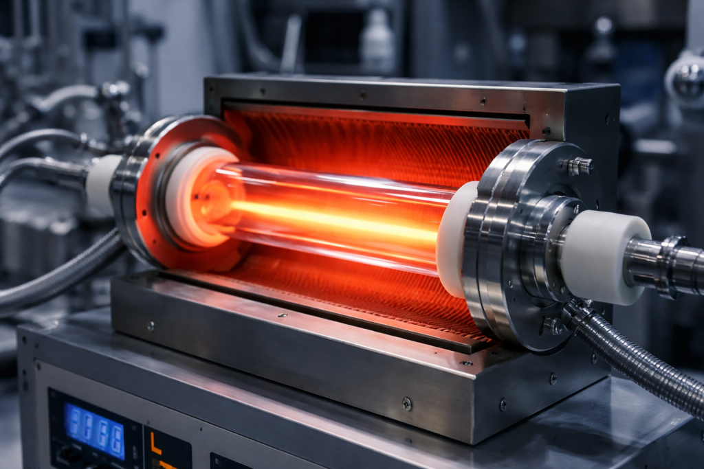
8-inch quartz wafers are increasingly used in semiconductor processing, MEMS, optical devices, wafer-level packaging, plasma systems, research equipment, and other applications that require high-purity, thermally stable, electrically insulating substrates.
Compared with conventional silicon wafers, fused quartz and fused silica wafers offer excellent chemical resistance, very low thermal expansion, good optical transmission, and high electrical insulation. However, specifying an 8-inch quartz wafer involves much more than simply requesting a nominal 200 mm diameter.
For precision applications, buyers should clearly define parameters such as diameter, thickness, thickness tolerance, TTV, flatness, bow, warp, surface roughness, edge profile, and polishing condition.
This guide explains the major specifications to consider when purchasing 8-inch quartz wafers and how each parameter can affect wafer handling, processing, bonding, coating, and final device performance.
What Is an 8-Inch Quartz Wafer?
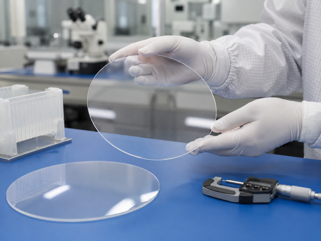
An 8-inch quartz wafer generally refers to a circular fused quartz or fused silica substrate with a diameter of approximately 200 mm.
Depending on the application, the wafer may be manufactured from:
- High-purity fused quartz
- Synthetic fused silica
- Optical-grade fused silica
- Semiconductor-grade quartz glass
Although these materials are often grouped together under the term “quartz wafer,” their chemical purity, OH content, optical transmission, thermal history, and manufacturing methods may differ.
Therefore, the material grade should always be specified together with dimensional requirements.
Typical 8-inch quartz wafer applications include:
- Semiconductor process monitoring
- MEMS manufacturing
- Wafer bonding
- Optical device fabrication
- Plasma processing
- Thin-film deposition
- Photolithography
- Sensor substrates
- Microfluidics
- Advanced packaging
- Research and development
1. Wafer Diameter
Diameter is one of the first specifications that should be defined.
An 8-inch quartz wafer is commonly described as a 200 mm wafer, but buyers should not assume that every supplier uses exactly the same dimensional standard.
The drawing or purchase specification should clearly state:
Nominal diameter: 200 mm
Diameter tolerance: according to the process requirement
The required tolerance depends on how the wafer will be handled.
For example, diameter accuracy may become important when the wafer must fit:
- Wafer carriers
- Vacuum chucks
- Spin coaters
- Lithography equipment
- Wafer bonding tools
- CMP equipment
- Cassette systems
- Inspection platforms
If the wafer is only used as a general laboratory substrate, a wider diameter tolerance may be acceptable.
For semiconductor equipment compatibility, tighter dimensional control may be required.
2. Quartz Wafer Thickness
Thickness has a major influence on mechanical strength, handling, thermal behavior, and compatibility with processing equipment.
8-inch quartz wafers can be manufactured in different thickness ranges depending on the application.
Common applications may require:
- Thin wafers for optical or MEMS processing
- Medium-thickness wafers for general semiconductor processing
- Thick quartz substrates for mechanical stability
- Custom thicknesses for bonding or carrier-wafer applications
Rather than simply specifying “standard thickness,” buyers should provide the actual target value.
For example:
Thickness: 1.0 mm
or
Thickness: 725 μm
depending on the equipment and process.
Why Thickness Matters
Wafer thickness affects several important characteristics.
Mechanical Strength
A thinner quartz wafer is more susceptible to:
- Breakage
- Edge damage
- Handling stress
- Vacuum chuck deformation
A thicker wafer is mechanically stronger, but it may not fit equipment designed around standard semiconductor wafer thicknesses.
Thermal Behavior
Quartz has a very low coefficient of thermal expansion, but wafer thickness still influences thermal mass.
A thicker wafer may:
- Heat more slowly
- Cool more slowly
- Provide better structural stability
A thinner wafer may respond more quickly during thermal processing.
Equipment Compatibility
Automatic equipment may have limitations related to:
- Wafer thickness
- Edge gripping
- Robot handling
- Vacuum chuck height
- Cassette spacing
Always confirm thickness compatibility before ordering wafers for automated processing.
3. Thickness Tolerance
Nominal thickness and thickness tolerance are different specifications.
For example, a wafer may be specified as:
1.00 mm ±0.05 mm
The first value defines the target thickness, while the second defines the allowable deviation.
Tighter thickness tolerances normally require additional grinding, lapping, and inspection.
For many applications, excessive thickness precision provides little benefit.
However, tight thickness control may be important for:
- Wafer bonding
- Optical path control
- Mechanical spacing
- Lithography equipment
- Multi-wafer stacking
- Precision fixtures
Buyers should therefore distinguish between nominal thickness tolerance and total thickness variation.
4. What Is TTV?
TTV means Total Thickness Variation.
It describes the difference between the maximum and minimum thickness measured across the wafer.
In simple terms:
TTV = Maximum Thickness − Minimum Thickness
For example, if the thickest measured point is 1.002 mm and the thinnest point is 0.994 mm:
TTV = 8 μm
TTV is one of the most important geometric specifications for precision quartz wafers.
Why TTV Matters
Low TTV helps provide more uniform wafer geometry.
This can improve performance in processes such as:
- Wafer bonding
- Photolithography
- Thin-film deposition
- CMP
- Vacuum chucking
- Optical processing
- Precision alignment
High TTV may result in uneven contact between the wafer and processing equipment.
It can also affect:
- Focus uniformity
- Bonding gap
- Coating uniformity
- Mechanical loading
For semiconductor and advanced optical applications, TTV should therefore be specified separately from average thickness.
5. Flatness
Flatness describes how closely the wafer surface corresponds to an ideal plane.
A wafer can have relatively uniform thickness while still being curved or distorted.
Therefore:
Low TTV does not automatically mean excellent flatness.
Flatness becomes especially important when the quartz wafer is used for:
- Lithography
- Wafer bonding
- Optical contact
- Precision coating
- Metrology
- Vacuum chuck mounting
Large-diameter quartz wafers can be more challenging to maintain at extremely tight flatness specifications because the entire 200 mm surface must be controlled.
6. TTV vs Flatness
TTV and flatness are sometimes confused, but they describe different characteristics.
| Specification | What It Measures |
|---|---|
| Thickness | Average wafer thickness |
| Thickness tolerance | Allowable deviation from nominal thickness |
| TTV | Variation in thickness across the wafer |
| Flatness | Deviation of a surface from an ideal plane |
| Bow | Overall curvature of the wafer |
| Warp | Total shape distortion across the wafer |
All of these parameters may be relevant for a high-precision quartz wafer.
For general laboratory applications, buyers may not need to specify all of them.
For semiconductor applications, however, clearly defining wafer geometry can help prevent processing problems.
7. Wafer Bow
Bow describes the overall curvature of the wafer relative to a reference plane.
A wafer may curve upward or downward even when its thickness is relatively uniform.
Excessive bow can affect:
- Vacuum chucking
- Wafer transfer
- Coating uniformity
- Lithography
- Bonding
- Automated handling
Bow can be influenced by:
- Material stress
- Grinding
- Lapping
- Polishing
- Thermal processing
- Coating stress
When quartz wafers are used in high-precision processes, bow requirements should be considered together with TTV and warp.
8. Wafer Warp
Warp is another measurement used to describe wafer shape.
While bow represents overall curvature, warp considers more complex deviations from a reference plane.
A wafer with low TTV may still show unacceptable warp.
Warp may cause problems when:
- The wafer cannot sit evenly on a chuck
- Bonding surfaces fail to contact uniformly
- Lithography focus varies across the wafer
- Robotic handling becomes unstable
For advanced processing applications, buyers should provide both bow and warp limits where necessary.
9. Surface Roughness
Surface roughness is an important parameter for polished quartz wafers.
It is commonly expressed as Ra.
Surface roughness can influence:
- Wafer bonding
- Thin-film deposition
- Optical performance
- Particle adhesion
- Cleaning performance
- Surface contamination
- Device fabrication
A mechanically ground wafer may appear smooth to the eye but still have significantly higher roughness than a precision-polished wafer.
Ground vs Polished Quartz Wafers
Quartz wafers can be supplied with different surface conditions.
Ground Surface
Ground wafers may be suitable for:
- Mechanical support
- Furnace fixtures
- General laboratory use
- Carrier applications where optical quality is unnecessary
Grinding marks may remain visible.
Single-Side Polished Wafer
A single-side polished, or SSP, wafer has one polished surface and one non-polished or less-finished surface.
SSP quartz wafers may be useful when only one functional surface is required.
Double-Side Polished Wafer
A double-side polished, or DSP, quartz wafer has both major surfaces polished.
DSP wafers are commonly selected for applications requiring:
- High flatness
- Low surface roughness
- Optical transmission
- Wafer bonding
- Microfabrication
- Precision inspection
The required polishing condition should always be included in the RFQ.
10. Surface Roughness for Semiconductor Applications
For semiconductor or research-grade quartz wafers, buyers often require very smooth surfaces.
The exact Ra requirement should depend on the downstream process.
For example, applications involving:
- Direct bonding
- Thin-film deposition
- Photolithography
- MEMS fabrication
- Optical coatings
may require significantly better surface quality than a quartz wafer used only as a mechanical support.
Instead of requesting the lowest possible Ra value, buyers should specify a realistic requirement based on their process.
Extremely low roughness may require additional polishing and inspection, which increases manufacturing cost.
11. Surface Quality and Scratch-Dig
For optical applications, surface roughness alone may not fully describe wafer quality.
Visible defects may include:
- Scratches
- Digs
- Pits
- Polishing marks
- Stains
- Surface contamination
Optical quartz wafers may therefore include a scratch-dig requirement.
Semiconductor applications may use different visual inspection criteria.
It is important to distinguish between:
Surface roughness
and
Visible surface defects.
A surface may have low Ra but still contain an unacceptable scratch.
12. Edge Profile
The wafer edge is important because quartz is a brittle material.
A sharp, unprocessed edge can be vulnerable to:
- Chipping
- Microcracks
- Breakage during handling
- Damage during transport
Typical quartz wafer edge treatments may include:
- Beveled edge
- Rounded edge
- Chamfered edge
- Ground edge
- Polished edge
The appropriate profile depends on the wafer thickness and handling process.
For automatic semiconductor equipment, edge geometry should be compatible with the handling system.
13. Edge Chipping
Edge chipping should be controlled during manufacturing and inspection.
Small chips may develop during:
- Coring
- Grinding
- Edge shaping
- Polishing
- Cleaning
- Packaging
For critical applications, buyers may specify:
- Maximum chip size
- Maximum chip depth
- Edge exclusion zone
- No cracks
- No major edge defects
An edge exclusion requirement can prevent small edge defects from affecting the active area of the wafer.
14. Edge Exclusion
Edge exclusion refers to a specified peripheral area of the wafer that is excluded from certain surface or inspection requirements.
For example, a process may define a small region near the outer edge where:
- Surface defects are evaluated differently
- Coating uniformity is not guaranteed
- Device structures are not placed
- Measurement data are excluded
Buyers should define edge exclusion if it affects inspection or device fabrication.
This is especially useful when comparing wafers from different suppliers because measurement areas must be consistent.
15. Quartz Wafer Purity
For semiconductor applications, dimensional specifications are only part of the requirement.
Material purity can also be critical.
Potential contaminants may include:
- Sodium
- Potassium
- Iron
- Aluminum
- Calcium
- Other metallic impurities
High-purity quartz materials are often selected to minimize contamination during high-temperature or plasma processing.
When purity is important, the RFQ should state:
- Required material grade
- Maximum impurity limits if applicable
- Semiconductor-grade requirement
- Certificate or analysis requirement
16. OH Content
OH content can influence the optical and thermal properties of fused silica.
Different manufacturing processes can produce materials with different hydroxyl concentrations.
Depending on the application, OH content may affect:
- Infrared transmission
- UV performance
- Thermal behavior
- Optical absorption
For ordinary mechanical wafer applications, OH content may not be critical.
For optical, laser, or specialized semiconductor applications, it may need to be controlled.
17. Optical Transmission
Quartz and fused silica wafers are often selected because of their excellent optical properties.
Depending on material grade, they may provide transmission across UV, visible, and infrared wavelength ranges.
When optical performance is important, buyers should specify:
- Operating wavelength
- Transmission requirement
- Material grade
- Surface polish
- Surface quality
Simply requesting “transparent quartz” does not provide enough information for a precision optical application.
18. Cleaning Requirements
Quartz wafers used in semiconductor manufacturing may require controlled cleaning after machining and polishing.
Potential contamination sources include:
- Grinding residues
- Polishing compounds
- Particles
- Fingerprints
- Metallic contamination
- Packaging debris
Depending on the application, cleaning may involve specialized chemical and ultrapure-water processes.
The RFQ should state whether the wafer requires:
- General industrial cleaning
- Precision cleaning
- Semiconductor-grade cleaning
- Cleanroom packaging
19. Packaging of 8-Inch Quartz Wafers
Large quartz wafers are vulnerable to mechanical damage during transportation.
Packaging should help prevent:
- Edge impact
- Wafer-to-wafer contact
- Surface scratching
- Particle contamination
- Moisture exposure
Depending on wafer grade and quantity, packaging may include:
- Individual protective separators
- Wafer carriers
- Clean bags
- Foam protection
- Double-box packaging
- Cleanroom-compatible packaging
For high-value polished wafers, surface protection is especially important.
20. Typical 8-Inch Quartz Wafer Specification Checklist
A clear RFQ can significantly reduce quotation time.
Buyers should consider providing the following information:
| Parameter | Information to Specify |
|---|---|
| Material | Fused quartz / fused silica grade |
| Diameter | 200 mm or custom |
| Diameter tolerance | According to equipment requirement |
| Thickness | Target thickness |
| Thickness tolerance | Maximum allowable deviation |
| TTV | Maximum allowable value |
| Flatness | Required if applicable |
| Bow | Maximum allowable value |
| Warp | Maximum allowable value |
| Surface | SSP or DSP |
| Roughness | Ra requirement |
| Surface quality | Scratch/dig or visual defect criteria |
| Edge | Bevel, chamfer, rounded or polished |
| Edge exclusion | Required area if applicable |
| Purity | Standard or semiconductor grade |
| Cleaning | Standard or semiconductor clean |
| Packaging | Standard or cleanroom-compatible |
| Quantity | Prototype and production quantities |
A drawing should be provided whenever custom tolerances or special geometry are required.
21. Example of an 8-Inch Quartz Wafer RFQ
A practical RFQ may look like this:
Product: High-Purity Fused Quartz Wafer
Diameter: 200 mm
Thickness: 1.00 mm
Surface: Double-side polished
TTV: Specify maximum requirement
Bow: Specify maximum requirement
Warp: Specify maximum requirement
Surface Roughness: Specify required Ra
Edge: Beveled
Material: High-purity fused quartz
Cleaning: Semiconductor-grade cleaning
Packaging: Clean packaging
Quantity: 10 pcs prototype, followed by production volume
Providing this information is much more useful than simply requesting:
“Please quote 8-inch quartz wafers.”
22. Avoid Over-Specifying the Wafer
Very tight specifications can significantly increase manufacturing difficulty and price.
For example, requiring simultaneously:
- Extremely low TTV
- Extremely low bow
- Extremely low warp
- Ultra-low surface roughness
- Tight thickness tolerance
may require multiple precision grinding, lapping, polishing, and inspection processes.
Before setting specifications, engineers should identify which parameters actually affect device performance.
For some applications, thickness and roughness may be critical while bow is less important.
For others, TTV and flatness may be the primary requirements.
A balanced specification can reduce cost while maintaining functional performance.
23. How to Choose Between SSP and DSP Quartz Wafers
Choosing between single-side and double-side polishing depends on the process.
SSP May Be Suitable When:
- Only one side is used for deposition
- One surface is used for optical processing
- The backside does not require precision polishing
- Cost control is important
DSP May Be Preferred When:
- Both surfaces are functional
- High flatness is required
- The wafer is used for bonding
- Optical transmission through both surfaces is required
- Precision measurement is required
- Both sides undergo processing
DSP generally requires more manufacturing steps and therefore may cost more than SSP.
24. Why 8-Inch Quartz Wafer Geometry Matters in Semiconductor Processing
As wafer diameter increases, geometric control becomes more important.
A small variation across a 200 mm wafer can affect process uniformity over a relatively large area.
Potential consequences include:
- Non-uniform coating
- Poor vacuum contact
- Bonding defects
- Lithography focus problems
- Handling instability
- Inconsistent device performance
For this reason, semiconductor buyers should evaluate diameter, thickness, TTV, bow, warp, flatness, and roughness as a complete specification rather than as isolated values.
Conclusion
Purchasing an 8-inch quartz wafer requires more than specifying a 200 mm diameter.
For semiconductor, MEMS, optical, wafer-bonding, and advanced research applications, parameters such as thickness, TTV, flatness, bow, warp, surface roughness, polishing condition, and edge quality can directly affect downstream processing.
The most effective RFQ clearly identifies the parameters that are critical to the application.
For a typical precision quartz wafer project, buyers should provide:
200 mm diameter + thickness + TTV + bow/warp + surface roughness + SSP/DSP + edge profile + material grade + cleaning requirement + quantity.
This allows the manufacturer to evaluate feasibility, select the appropriate grinding and polishing process, and provide a more accurate quotation.
For custom 8-inch high-purity fused quartz wafers, especially those used in semiconductor, optical, MEMS, and wafer-level processing, early confirmation of wafer geometry and surface specifications can help improve manufacturing consistency and reduce unnecessary production cost.
Frequently Asked Questions
Is an 8-inch quartz wafer exactly 200 mm?
8-inch wafers are commonly referred to as 200 mm wafers. However, buyers should specify the exact nominal diameter and tolerance required for their equipment rather than relying only on the “8-inch” description.
What is TTV in a quartz wafer?
TTV means Total Thickness Variation. It is the difference between the maximum and minimum measured thickness across the wafer.
Is TTV the same as flatness?
No. TTV measures thickness variation, while flatness measures how much a wafer surface deviates from an ideal plane.
What is the difference between bow and warp?
Bow describes the overall curvature of the wafer, while warp describes more complex deviations in wafer shape. Both can affect chucking, bonding, lithography, and wafer handling.
Should I choose SSP or DSP quartz wafers?
SSP is often suitable when only one surface is functional. DSP is generally preferred for wafer bonding, optical applications, high-flatness requirements, or processes where both sides of the wafer are used.
What information should I provide when requesting a quote?
At minimum, provide the material grade, diameter, thickness, thickness tolerance, TTV, surface finish, roughness, edge requirement, cleaning requirement, quantity, and any required bow or warp limits.