
Tổng quan về sản phẩm
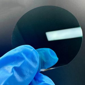
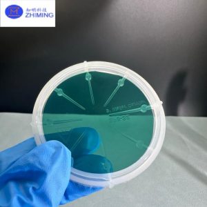
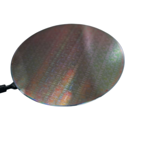
Lithium Niobate on Insulator (LNOI) wafers are advanced thin-film photonic materials fabricated by bonding a high-quality LiNbO₃ single crystal layer onto an insulating substrate (such as Si or SiO₂).
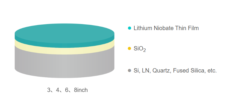
By combining ion implantation + wafer bonding + smart-cut technology, LNOI enables ultra-thin lithium niobate films with excellent optical and electrical performance.
It is widely used in:
- High-speed electro-optic modulators
- RF acoustic wave filters (SAW/BAW)
- Integrated photonics circuits
- Quantum optical devices
- High-frequency communication systems
Những ưu điểm nổi bật
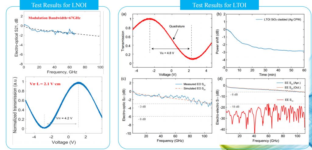
1. High-Speed & Low Power Optical Performance
- Ultra-high bandwidth electro-optic modulation
- High transmission rate
- Low driving voltage
- Small device footprint → supports photonic integration
2. RF & 5G Communication Advantages
- High electromechanical coupling coefficient (Ke² > 25%)
- Wide bandwidth acoustic wave response
- Excellent high-frequency performance
- Suitable for next-generation 5G/6G RF filters
3. Excellent Stability & Reliability
- Strong temperature stability
- High chemical resistance (acid & alkali resistant)
- Stable operation under harsh environments
- High heat dissipation capability
4. Superior Material Properties of LiNbO₃
- Strong electro-optic (Pockels) effect
- Excellent piezoelectric properties
- Nonlinear optical performance
- High compatibility with integrated photonics
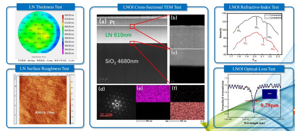
Công nghệ sản xuất
LNOI wafers are produced using Smart-Cut + Wafer Bonding Process:
 He ion implantation
- Helium ions implanted into LiNbO₃ crystal
- Creates controlled weak cleavage layer
-
Wafer bonding
- Bonded to Si or SiO₂ substrate under high temperature & pressure
- Thermal annealing
- Defect evolution and layer separation
- Forms high-quality thin film LiNbO₃ layer
- Surface finishing
- Polishing and thinning to required nanometer-micrometer thickness
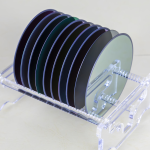
Typical Specifications
| Item | Thông số kỹ thuật |
|---|---|
| Wafer Size | 150 mm ±0.2 mm |
| Film Thickness | 350 nm – few µm (customizable) |
| Orientation | X-cut / Y-cut ±0.2° |
| Surface Roughness | Ra ≤ 0.5 nm (AFM RMS) |
| TTV | < 70 µm (150 mm wafer) |
| Độ phẳng | < 1.3 µm |
| Sự minh bạch | >95% (450–700 nm) |
| Curie Temperature | 1142 ±1°C |
Ứng dụng
1. Integrated Photonics
- Optical modulators
- Waveguides
- Resonators
- On-chip photonic circuits
2. Telecom & Data Center
- High-speed fiber communication
- Optical signal modulation
- Data center interconnect (DCI)
3. RF & Wireless Communication
- SAW/BAW RF filters
- 5G/6G high-frequency devices
- Low-loss RF components
4. Quantum & Advanced Optics
- Entangled photon generation
- Quantum communication systems
- Nonlinear optics devices
5. Sensors & MEMS
- Pressure sensors
- Acceleration sensors
- Acoustic and vibration devices
Why LNOI Matters
Compared with traditional bulk lithium niobate:
- Smaller device size
- Higher bandwidth
- Easier photonic integration
- Lower power consumption
- CMOS-compatible platform potential
It is a key material for next-generation photonics + RF convergence technology.
Đánh giá
Chưa có đánh giá nào.