
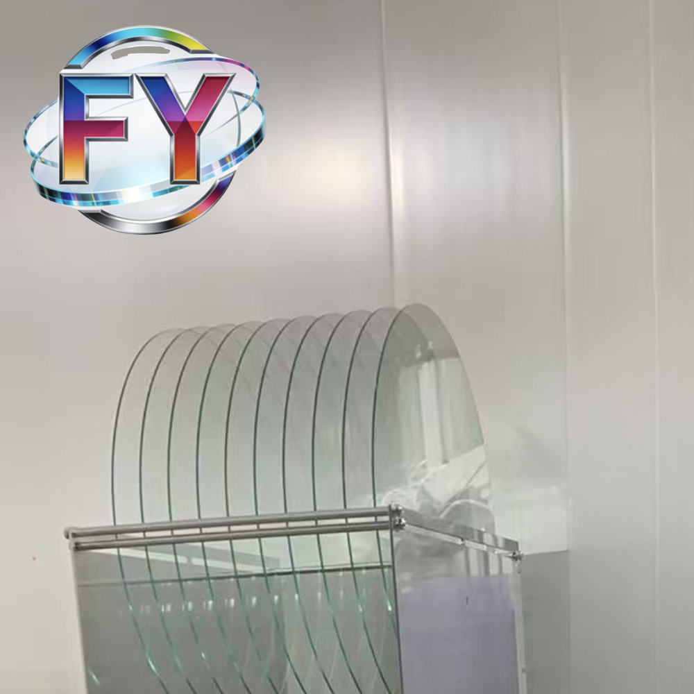
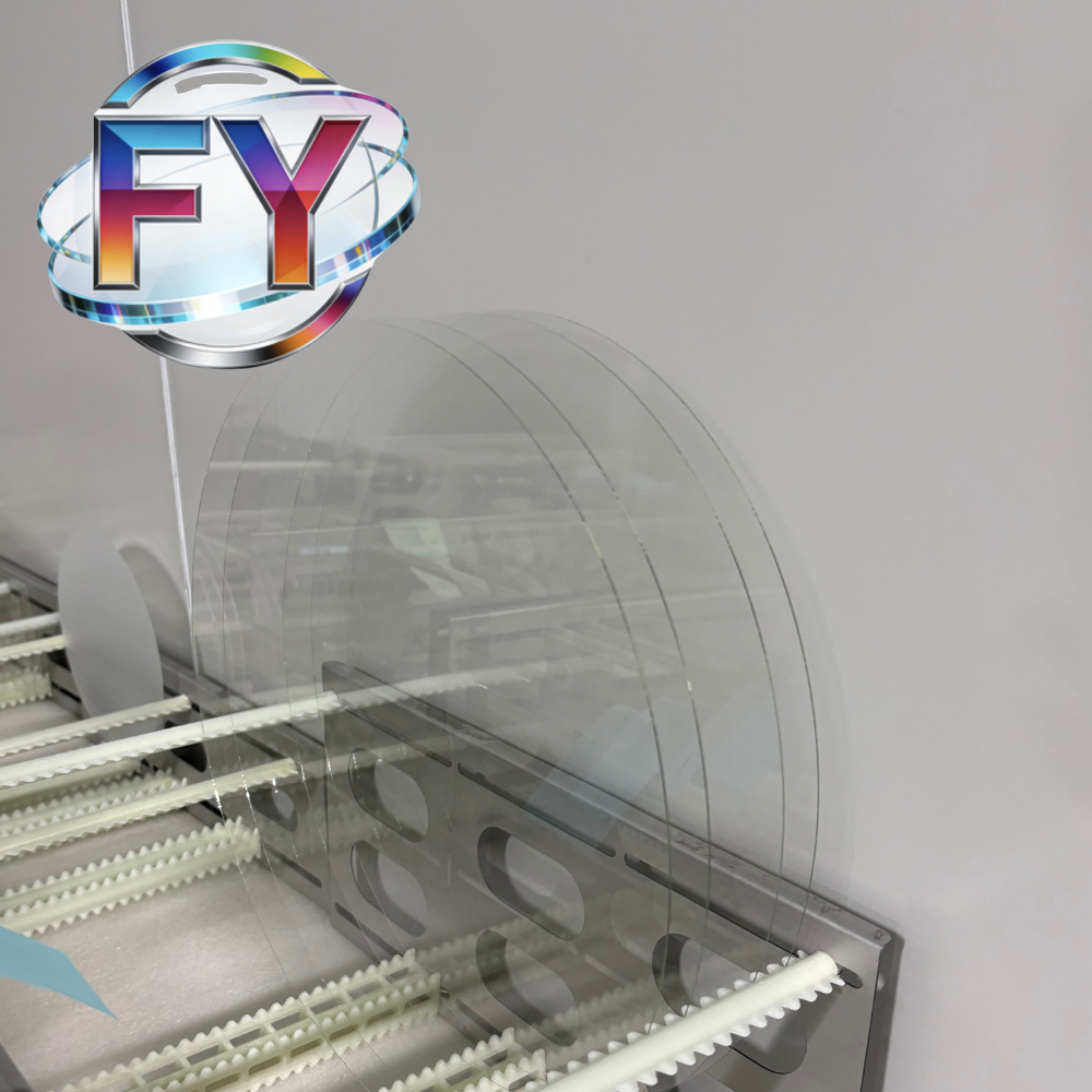

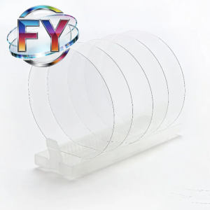
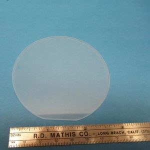
 12-inch Glass Substrates are emerging as a next-generation platform material for advanced semiconductor packaging, AI processors, high-performance computing (HPC), photonic integration, and Through-Glass Via (TGV) technologies.
Compared with traditional organic substrates and silicon-based platforms, glass substrates offer superior dimensional stability, excellent electrical insulation, low dielectric loss, and high optical transparency. These characteristics make glass an attractive solution for future semiconductor packaging architectures that require larger package sizes, higher interconnect density, and improved signal integrity.
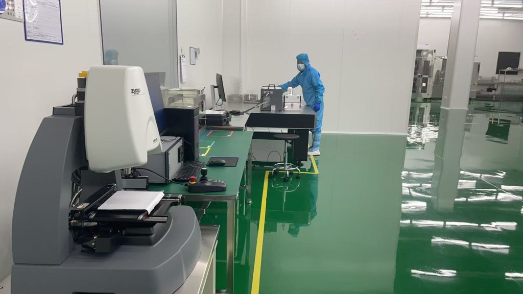
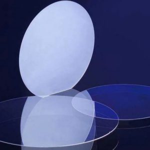
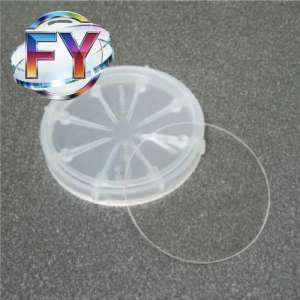
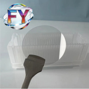
Our 12-inch (300 mm) Glass Substrates are manufactured to semiconductor-grade standards and are available in various glass materials, thicknesses, and surface finishes to support both R&D and volume production requirements.
 Fő jellemzők
- Standard 300 mm (12-inch) substrate format
- Kiváló méretstabilitás
- Low dielectric constant and signal loss
- High electrical insulation performance
- Outstanding surface flatness
- Nagy optikai átláthatóság
- Compatible with TGV processing
- Suitable for large-format package architectures
- Available with double-side polishing (DSP)
- Custom machining and processing available
Műszaki specifikációk
| Paraméter | Specifikáció |
|---|---|
| Átmérő | 300 mm (12 Inch) |
| Material Options | Borosilicate Glass, Aluminosilicate Glass, Fused Silica, Quartz Glass |
| Vastagságtartomány | 100 μm – 2000 μm |
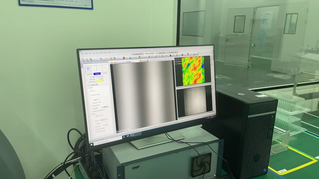
| Felületkezelés | SSP / DSP |
| Felületi érdesség | Személyre szabott |
| TTV | Személyre szabott |
| Bow & Warp | Személyre szabott |
| Edge Profile | Rounded Edge / Chamfered Edge |
| Optikai átvitel | High Transparency |
| Feldolgozási szolgáltatások | TGV, Laser Drilling, Metallization, Coating, Dicing |
Alkalmazások
Advanced Semiconductor Packaging
Glass substrates are increasingly used in advanced packaging technologies including:
- Chiplet Packaging
- Fan-Out Packaging
- 2.5D Integration
- 3D Integration
- Wafer-Level Packaging (WLP)
- Heterogén integráció
Their excellent dimensional stability supports fine-line redistribution layers and high-density interconnect structures.
Through-Glass Via (TGV)
Glass substrates provide an ideal platform for TGV fabrication, enabling vertical electrical connections with excellent insulation and low signal loss.
AI and High-Performance Computing
As AI accelerators and HPC devices continue to increase in complexity and package size, glass substrates are becoming an important enabling material for next-generation package architectures.
Silicon Photonics
The optical properties of glass make it suitable for photonic integrated circuits, optical communication modules, and advanced optical interconnect technologies.
MEMS and Sensor Devices
Glass substrates are widely utilized in MEMS fabrication, microfluidic systems, optical sensors, and precision electronic devices.
Advantages of Glass Substrates
Excellent Electrical Performance
Glass exhibits low dielectric loss and excellent insulation properties, helping improve signal integrity in high-frequency and high-speed applications.
Superior Dimensional Stability
Compared with organic substrate materials, glass offers enhanced flatness and reduced deformation during semiconductor processing.
Support for Large-Scale Integration
The 12-inch substrate format enables larger package designs and higher interconnect density required by advanced computing systems.
Future-Oriented Packaging Platform
Glass substrates are widely regarded as one of the key enabling technologies for next-generation semiconductor packaging beyond conventional organic substrates.
Testreszabási lehetőségek
We offer a comprehensive range of custom manufacturing services, including:
- Precision grinding and thinning
- Double-side polishing (DSP)
- Through-Glass Via (TGV) support
- Lézeres fúrás
- Precision dicing
- Metallizálás
- Thin substrate handling
- Optikai bevonatok
- Custom edge processing
GYIK
Why are glass substrates gaining attention in advanced packaging?
Glass substrates provide superior dimensional stability, low dielectric loss, and compatibility with TGV technology, making them highly suitable for next-generation semiconductor packaging.
Can 12-inch glass substrates support TGV processing?
Yes. Glass substrates are one of the primary platform materials used for Through-Glass Via technology and advanced interposer applications.
What glass materials are available?
Available materials typically include borosilicate glass, aluminosilicate glass, fused silica, and quartz glass. Material selection can be customized according to thermal, electrical, and optical requirements.
Értékelések
Még nincsenek értékelések.