

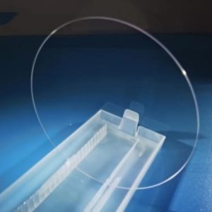
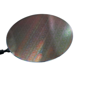
 12-дюймовые стеклянные подложки становятся материалом нового поколения для передовых технологий упаковки полупроводников, процессоров искусственного интеллекта, высокопроизводительных вычислений (HPC), фотонной интеграции и технологий сквозных стеклянных переходных отверстий (TGV).
По сравнению с традиционными органическими подложками и платформами на основе кремния стеклянные подложки обладают превосходной стабильностью размеров, отличной электрической изоляцией, низкими диэлектрическими потерями и высокой оптической прозрачностью. Эти характеристики делают стекло привлекательным решением для будущих архитектур корпусов полупроводниковых устройств, требующих увеличения размеров корпусов, повышения плотности межсоединений и улучшения целостности сигнала.
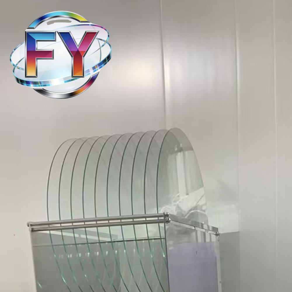
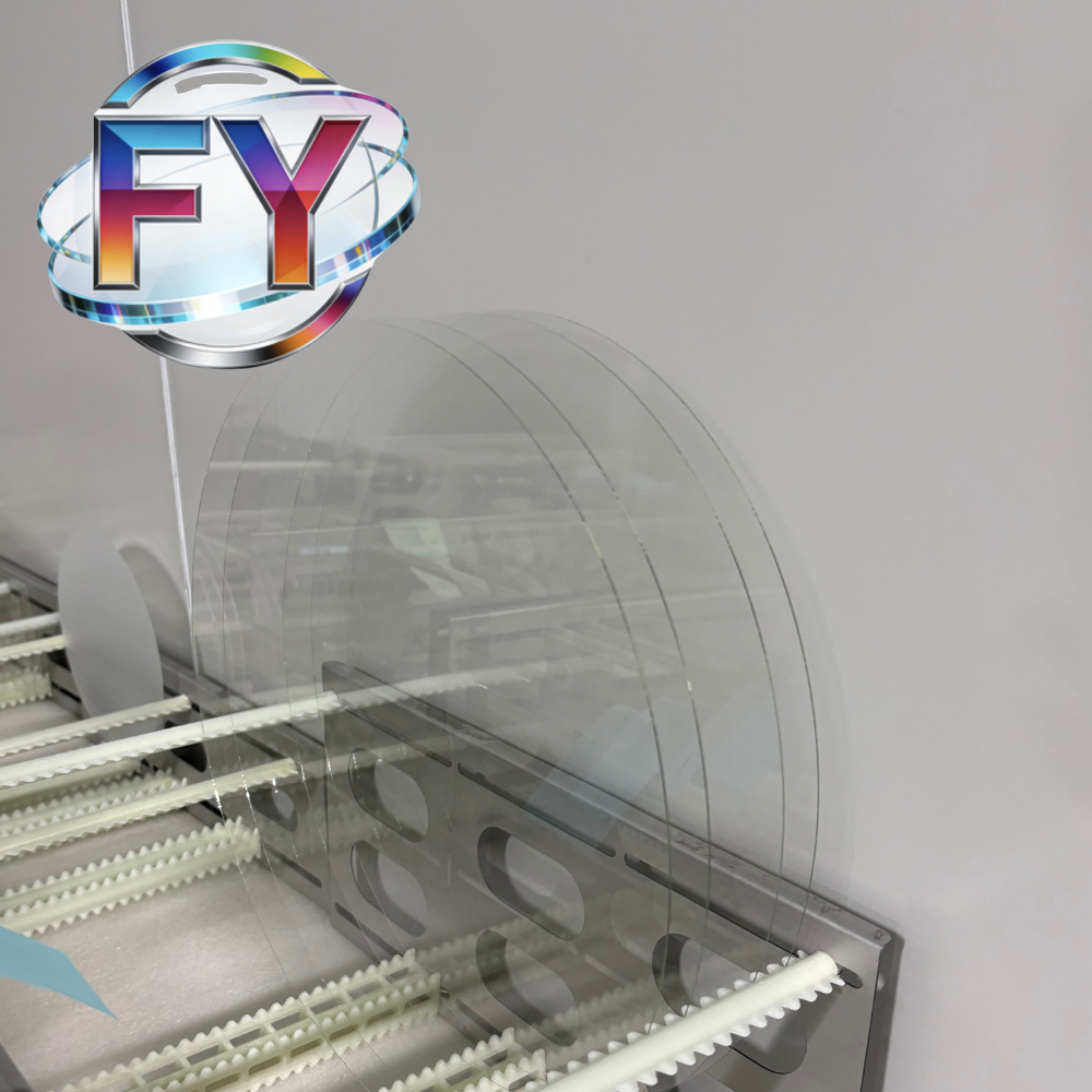
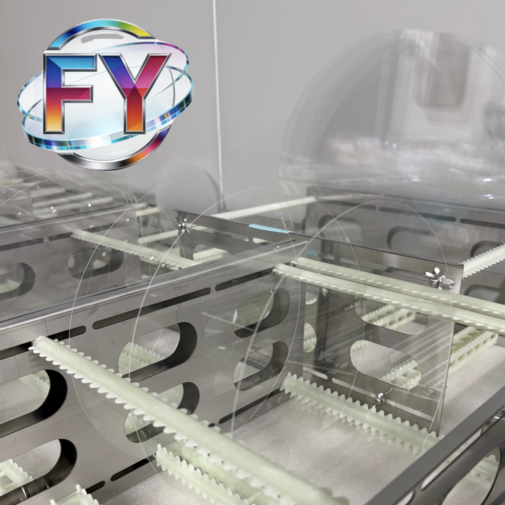
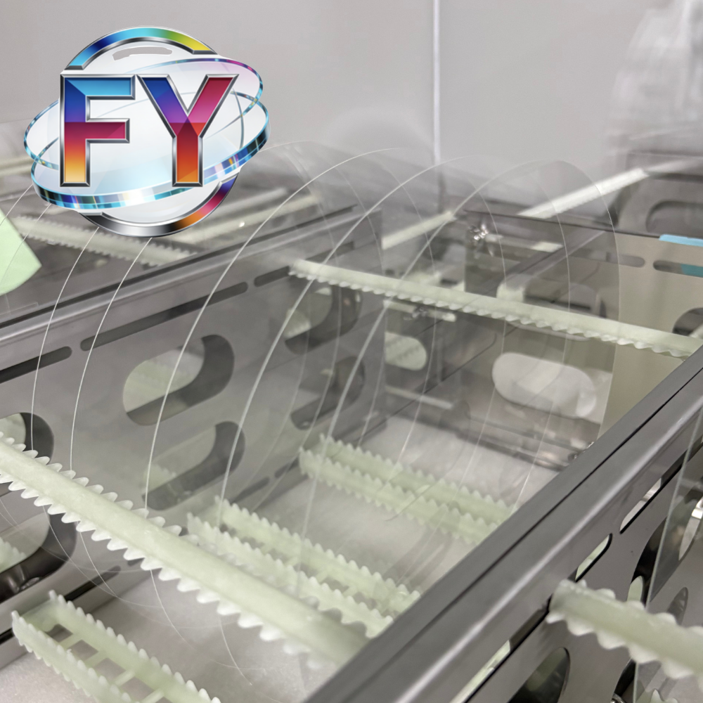
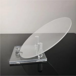
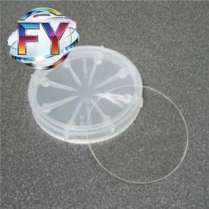
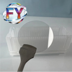
Наши стеклянные подложки диаметром 12 дюймов (300 мм) изготавливаются в соответствии со стандартами полупроводниковой промышленности и предлагаются с различными видами стекла, толщиной и типом поверхности, что позволяет удовлетворить как потребности научно-исследовательских и опытно-конструкторских работ, так и требования серийного производства.
 Основные характеристики
- Стандартный формат подложки 300 мм (12 дюймов)
- Отличная стабильность размеров
- Низкая диэлектрическая проницаемость и потери сигнала
- Высокие характеристики электрической изоляции
- Превосходная плоскостность поверхности
- Высокая оптическая прозрачность
- Совместимо с обработкой TGV
- Подходит для архитектур упаковок большого формата
- Предлагается с двусторонней полировкой (DSP)
- Возможна обработка и изготовление по индивидуальному заказу
Технические характеристики
| Параметр | Технические характеристики |
|---|---|
| Диаметр | 300 мм (12 дюймов) |
| Варианты материалов | Боросиликатное стекло, алюмосиликатное стекло, плавленый кремнезем, кварцевое стекло |
| Диапазон толщины | 100 мкм – 2000 мкм |
| Отделка поверхности | SSP / DSP |
| Шероховатость поверхности | Индивидуальный |
| TTV | Индивидуальный |
| Узел и основа | Индивидуальный |
| Профиль кромки | Закруглённый край / Скошенный край |
| Оптическая передача | Высокая прозрачность |
| Услуги по обработке данных | TGV, лазерное сверление, металлизация, нанесение покрытий, резка на кристаллы |
Приложения
Передовые технологии упаковки полупроводников
Стеклянные подложки всё чаще используются в передовых технологиях упаковки, в том числе:
- Компоновка чиплетов
- Распределительная упаковка
- 2,5D-интеграция
- 3D-интеграция
- Упаковка на уровне пластин (WLP)
- Гетерогенная интеграция
Их превосходная стабильность размеров позволяет создавать слои с тонкой линией перераспределения и структуры межсоединений высокой плотности.
Сквозное соединение через стекло (TGV)
Стеклянные подложки служат идеальной основой для изготовления TGV, обеспечивая вертикальные электрические соединения с превосходной изоляцией и низкими потерями сигнала.
Искусственный интеллект и высокопроизводительные вычисления
По мере того как ускорители на базе искусственного интеллекта и устройства для высокопроизводительных вычислений (HPC) становятся всё более сложными, а размеры их корпусов — всё больше, стеклянные подложки приобретают всё большее значение в качестве материала, обеспечивающего реализацию архитектур корпусов следующего поколения.
Кремниевая фотоника
Благодаря своим оптическим свойствам стекло подходит для использования в фотонных интегральных схемах, модулях оптической связи и передовых технологиях оптических соединений.
MEMS и сенсорные устройства
Стеклянные подложки широко используются при изготовлении МЭМС, в микрофлюидных системах, оптических датчиках и прецизионных электронных устройствах.
Преимущества стеклянных подложек
Превосходные эксплуатационные характеристики электрооборудования
Стекло характеризуется низкими диэлектрическими потерями и превосходными изоляционными свойствами, что способствует повышению целостности сигнала в высокочастотных и высокоскоростных системах.
Превосходная стабильность размеров
По сравнению с органическими материалами-подложками стекло обеспечивает более высокую плоскостность и меньшую деформацию в процессе производства полупроводников.
Поддержка крупномасштабной интеграции
12-дюймовый формат подложки позволяет создавать корпуса больших размеров и обеспечивать более высокую плотность межсоединений, что необходимо для современных вычислительных систем.
Перспективная платформа для упаковки
Стеклянные подложки широко считаются одной из ключевых технологий, открывающих путь к созданию полупроводниковых корпусов нового поколения, выходящих за рамки традиционных органических подложек.
Возможности персонализации
Мы предлагаем полный спектр услуг по изготовлению продукции на заказ, в том числе:
- Прецизионное шлифование и снятие слоя
- Двусторонняя полировка (DSP)
- Поддержка сквозных переходов через стекло (TGV)
- Лазерное сверление
- Точная нарезка
- Металлизация
- Обработка тонких подложек
- Оптические покрытия
- Настраиваемая обработка краев
ЧАСТО ЗАДАВАЕМЫЕ ВОПРОСЫ
Почему стеклянные подложки привлекают внимание в сфере передовых технологий упаковки?
Стеклянные подложки отличаются превосходной стабильностью размеров, низкими диэлектрическими потерями и совместимостью с технологией TGV, что делает их идеальным выбором для корпусов полупроводниковых устройств нового поколения.
Могут ли 12-дюймовые стеклянные подложки использоваться в технологическом процессе TGV?
Да. Стеклянные подложки являются одним из основных материалов, используемых в технологии сквозных сквозных переходов (Through-Glass Via) и в передовых решениях с использованием промежуточных слоев.
Какие виды стекла доступны?
К доступным материалам обычно относятся боросиликатное стекло, алюмосиликатное стекло, плавленый диоксид кремния и кварцевое стекло. Выбор материала может быть адаптирован с учетом тепловых, электрических и оптических требований.
Отзывы
Отзывов пока нет.