
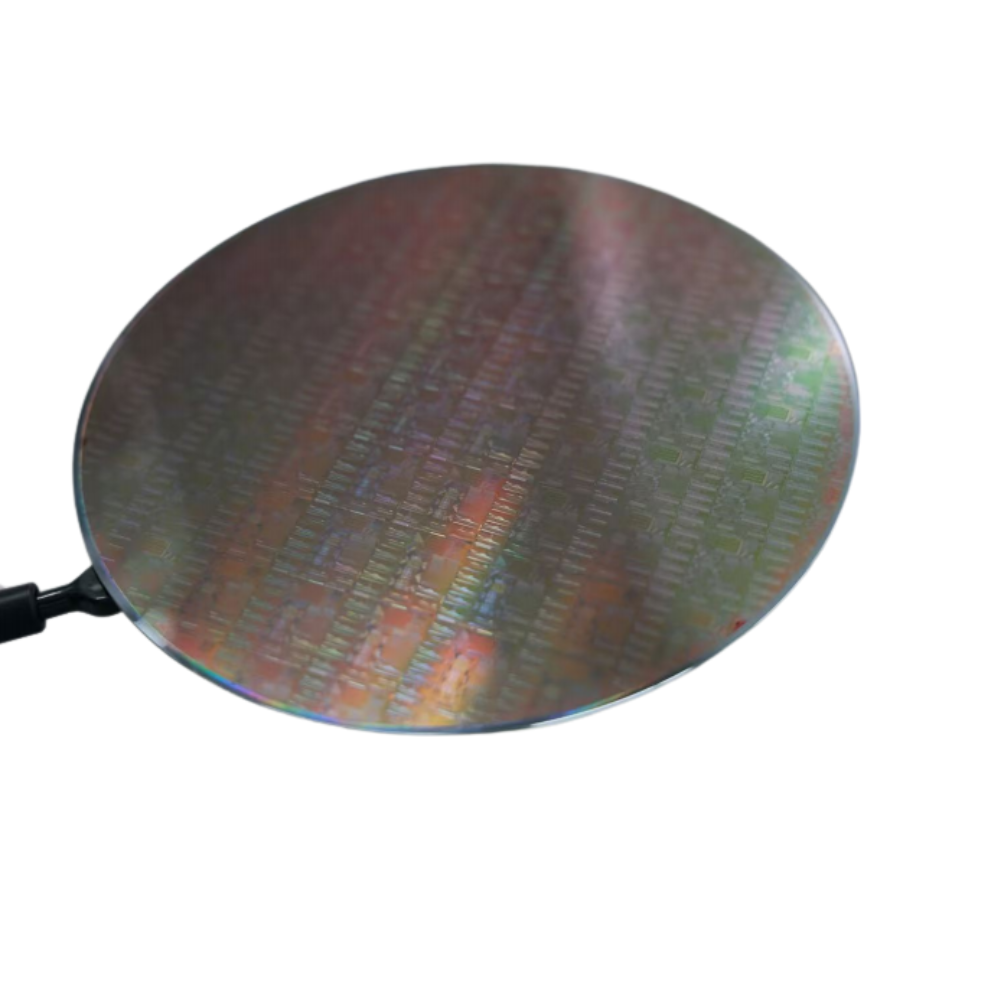
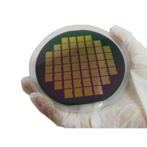
Přehled produktů
TFLN (Thin-Film Lithium Niobate) a TFLT (Thin-Film Lithium Tantalate) na křemíkové fotonice (SiPh) představují pokročilou heterogenní integrační platformu vyvinutou k překonání fyzikálních omezení křemíku ve fotonických systémech.
Křemíková fotonika nabízí vynikající nt škálovatelnost a kompatibilitu s CMOS, ale postrádá silný lineární elektrooptický (Pockelsův) efekt a trpí relativně vysokými ztrátami a omezenou linearitou modulace. K řešení těchto omezení se na platformy SiPh zavádějí tenkovrstvé LiNbO₃ a LiTaO₃ prostřednictvím lepení na destičky nebo technik hybridní integrace.
Toto řešení umožňuje kombinovat:
- Vysokorychlostní elektrooptický výkon TFLN/TFLT
- Možnost rozsáhlé integrace z křemíkové fotoniky
Má široké využití v optických propojeních nové generace, koherentních komunikačních systémech a mikrovlnné fotonice.
Definice základního materiálu
TFLN (tenkovrstvý lithium-niobát)
Tenkovrstvý niobát lithia poskytuje silný Pockelsův efekt, který umožňuje velmi rychlou optickou modulaci s nízkými vložnými ztrátami. V současné době je průmyslovým standardem pro vysokorychlostní optické modulátory.
TFLT (tenkovrstvý tantalát lithný)
Tenkovrstvý tantalát lithný vykazuje podobné elektrooptické chování, ale nabízí lepší tepelnou stabilitu, vyšší práh optického poškození a lepší rovnoměrnost na úrovni destičky. Je považován za slibnou alternativu pro výkonné a rozsáhlé aplikace.
 Proč integrovat TFLN / TFLT s křemíkovou fotonikou?
Samotný křemík nemůže účinně podporovat vysoce výkonnou modulaci kvůli:
- Absence vlastního elektrooptického efektu
- Závislost na disperzním efektu plazmatu, který vede k vyšším optickým ztrátám
- Omezená linearita pro pokročilé modulační formáty
Integrací TFLN/TFLT do SiPh platforma dosahuje:
- Šířka modulačního pásma přesahující 100 GHz, podpora systémů 800G a 1,6T
- Nižší půlvlnné napětí (Vπ), snížení spotřeby energie
- Velmi nízké optické ztráty šíření
- Široké okno průhlednosti od viditelného až po střední infračervené pásmo
Integrační přístupy
1. Heterogenní integrace (metoda lepení)
Tenkovrstvý LN nebo LT se lepí na předem vyrobené vlnovody z křemíku nebo nitridu křemíku (Si/SiN).
- Optická vazba prostřednictvím evanescentního pole
- zachovává plnou kompatibilitu s výrobou křemíkové fotoniky
- Vhodné pro velkovýrobu
2. Vlnovodný přístup LNOI / LTOI
Vlnovody jsou vyleptány přímo do tenkovrstvé vrstvy LN nebo LT.
- Silné optické omezení v monokrystalickém materiálu
- Nejvyšší účinnost modulace
- Složitější výroba a nižší kompatibilita se standardními procesy SiPh
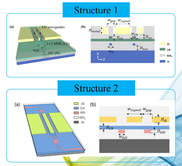
Typická struktura (doporučené umístění obrázku)
Struktura 1: Hybridní vlnovod (SiPh + TFLN/TFLT)
- Si nebo SiN vlnovod (spodní vrstva)
- Vazebná vrstva SiO₂
- Tenkovrstvá vrstva LN/LT (~300-600 nm)
- RF elektrody na horní straně
Struktura 2: Hřebenový vlnovod (LNOI/LTOI)
- LN/LT tenká vrstva
- Pohřbený oxid (BOX)
- Křemíkový substrát
Parametry výkonu
| Parametr | TFLN | TFLT | Poznámky |
|---|---|---|---|
| Elektrooptický koeficient (r33) | ~31 pm/V | ~30 pm/V | Podobná účinnost modulace |
| Šířka pásma 3 dB | 100-400 GHz+ | 70-100 GHz+ | Mnohem vyšší než u Si modulátorů (~40 GHz) |
| Vπ-L | 1,8-2,5 V-cm | 2,0-3,5 V-cm | Nižší znamená nižší napětí pohonu |
| Optické ztráty | <0,1 dB/cm | <0,1 dB/cm | Extrémně nízká |
| Index lomu | ~2.1-2.2 | ~2.1 | Vysoká uzavírací schopnost |
| Curieho teplota | ~1140°C | ~600°C | Odkaz na vlastnost materiálu |
| Práh optického poškození | Mírná | Velmi vysoká | TFLT lepší pro vysoký výkon |
| Drift stejnosměrného proudu | Výrazné | Velmi nízká | TFLT má vynikající stabilitu |
Hlavní výhody
Možnost vysokorychlostní modulace
Podporuje optickou modulaci s velmi vysokou šířkou pásma přesahující 100 GHz, což umožňuje přenosové rychlosti nové generace.
Nízká spotřeba energie
Snížené půlvlnné napětí umožňuje nižší řídicí výkon ve srovnání s křemíkovými modulátory.
Vynikající optický výkon
Nízké ztráty šíření a vysoký index lomu umožňují kompaktní a efektivní fotonickou integraci.
Tepelná a výchylková stabilita (výhoda TFLT)
TFLT zajišťuje lepší odolnost vůči tepelným změnám a minimální drift stejnosměrného proudu, což je důležité pro dlouhodobou stabilitu systému.
Škálovatelná výroba
Integrace založená na lepení zachovává kompatibilitu s křemíkovými fotonickými procesy a podporuje výrobu v měřítku destiček.
Scénáře použití
- Optické propojení datových center (400G / 800G / 1,6T)
- Koherentní optické komunikační systémy
- Mikrovlnná fotonika a RF-over-fiber
- Integrované fotonické obvody (PIC)
- Vysoce výkonné laserové modulační systémy
- LiDAR a snímací platformy
Pokyny pro výběr
TFLN si vyberte, když:
- Je požadována maximální šířka modulačního pásma
- Preferuje se vyspělý ekosystém a dodavatelský řetězec.
- Cílové aplikace zahrnují koherentní optiku a ultrarychlý přenos.
Zvolte si TFLT, když:
- Stabilita výchylky a nízký stejnosměrný drift jsou kritické.
- Je vyžadován vysoký optický výkon
- Prioritou je dlouhodobá spolehlivost a tepelná odolnost
ČASTO KLADENÉ DOTAZY
1. Jaká je hlavní výhoda TFLN/TFLT na SiPh ve srovnání s křemíkovými modulátory?
Klíčovou výhodou je přítomnost silného elektrooptického efektu, který umožňuje větší šířku pásma, nižší ztráty a nižší spotřebu energie než u křemíkových modulátorů.
2. Jak funguje evanescentní vazba v hybridní integraci?
Světlo se šíří v křemíkovém vlnovodu a částečně zasahuje do tenkovrstvé vrstvy LN nebo LT. Toto překrývající se optické pole umožňuje účinnou modulaci bez úplného přenosu optického módu.
3. Je tato platforma vhodná pro velkovýrobu?
Ano. Heterogenní integrace založená na lepení umožňuje kompatibilitu se standardními procesy výroby křemíkové fotoniky, což umožňuje velkoobjemovou a nákladově efektivní výrobu.

Recenze
Zatím zde nejsou žádné recenze.