Artificial intelligence is no longer affecting only the chip-design market. It is reshaping semiconductor manufacturing capacity, memory investment and the global equipment supply chain.
The rapid expansion of AI data centers has created strong demand for high-performance GPUs and accelerators, but those processors also depend heavily on advanced memory—particularly High Bandwidth Memory (HBM).
As HBM3E production scales and HBM4 enters volume manufacturing, memory manufacturers are investing in new wafer fabrication capacity, advanced DRAM processes and additional production infrastructure.
According to SEMI’s latest 300mm Fab Outlook, global 300mm front-end fab equipment spending is projected to reach a record US$149 billion in 2026, up 31% year over year. Memory equipment spending alone is expected to increase approximately 32% in 2026, driven largely by AI-related memory demand.
This new investment cycle has implications far beyond lithography systems, deposition equipment or wafer-processing tools.
It is also expanding the installed base of process chambers, furnaces and wafer-handling systems that require high-purity consumable and replacement components.
Among them are high-purity fused quartz process components.
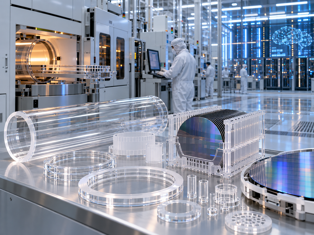
Quartz tubes, furnace tubes, wafer boats, carriers, rings, liners, plates, windows and custom fabricated quartz assemblies remain important components in many semiconductor manufacturing environments where high-temperature stability, chemical resistance and contamination control are required.
AI Is Creating a New Memory Investment Cycle
The rise of generative AI has significantly changed the role of memory in computing systems.
Traditional servers already require substantial DRAM capacity, but modern AI accelerators require much higher memory bandwidth to continuously move large amounts of data between memory and processing units.
HBM addresses this challenge by stacking multiple DRAM dies and connecting them through advanced interconnect technologies.
The result is substantially higher bandwidth than conventional memory configurations.
As AI models become larger and inference workloads expand, demand is growing not only for computing power but also for the memory infrastructure surrounding that compute capacity.
SEMI reported in June 2026 that worldwide 300mm fab equipment investment in the memory sector was expected to exceed US$50 billion for the first time, reaching approximately US$52 billion in 2026. DRAM equipment spending was projected at roughly US$37 billion, supported by demand for HBM and DDR5.
The latest Q3 outlook has since strengthened the broader semiconductor investment forecast, with global 300mm equipment spending now projected at US$149 billion for 2026.
This suggests that AI-related semiconductor demand is increasingly moving from forecasts and capacity planning into physical manufacturing investment.
HBM4 Is Moving Into Volume Production
The transition is also visible at the product level.
HBM4, the next generation following HBM3E, has already entered commercial production.
Micron announced in March 2026 that its 36GB 12-high HBM4 had entered high-volume production, with shipments beginning during the first quarter of the year. The company reported bandwidth exceeding 2.8 TB/s for the product.
SK hynix also reported that it began mass shipments of HBM4 during the second quarter of 2026 and planned to increase production during the second half of the year.
These developments matter because HBM growth is not simply about producing more memory chips.
Advanced HBM requires sophisticated DRAM wafer fabrication, tighter process control and complex downstream packaging.
For suppliers of semiconductor process components, the more relevant impact comes from the front-end DRAM capacity and technology migration needed to support these memory products.
More advanced DRAM production means additional equipment investment, more processing capacity and potentially greater demand for qualified process components.
Memory Manufacturers Are Expanding Physical Fab Capacity
The investment cycle is already leading to large-scale fab projects.
In August 2026, SK hynix announced investments totaling approximately 54 trillion Korean won across its Yongin Y2 and Cheongju M17 fabs. The company said the projects are intended to establish additional mid- to long-term production capacity for AI memory demand, covering both DRAM and NAND.
SK hynix has also begun construction of a more than US$4 billion HBM production base in Indiana, with next-generation HBM mass production in the United States targeted for the second half of 2029.
Micron is moving in a similar direction.
In July 2026, the company increased its planned U.S. semiconductor investments to more than US$250 billion through 2035, citing growing memory demand in the AI era.
Micron is also building an advanced wafer fabrication facility in Singapore with a planned investment of approximately US$24 billion over ten years. The fab is expected to provide roughly 700,000 square feet of cleanroom space, with wafer output scheduled to begin in the second half of 2028.
Taken together, these projects illustrate an important change in the semiconductor cycle:
AI demand is translating into cleanrooms, wafer capacity, equipment installations and physical manufacturing infrastructure.
What Does HBM Growth Have to Do With Quartz Components?
It is important to distinguish between HBM packaging itself and semiconductor front-end manufacturing.
A quartz furnace tube is not installed simply because an HBM stack contains more memory layers.
Instead, the relationship is indirect but important.
HBM demand encourages manufacturers to increase advanced DRAM production.
Increasing DRAM capacity requires additional wafer fabrication equipment.
Those tools support many individual processes, including thermal treatment, oxidation, diffusion, deposition, annealing, cleaning and other semiconductor manufacturing steps.
Many such environments use high-purity fused quartz components because quartz offers a useful combination of:
- High temperature resistance
- Low thermal expansion
- Good thermal shock resistance
- High chemical stability
- Low contamination potential when appropriate material grades are used
- Good optical transmission for selected applications
- Precision fabrication capability
- Compatibility with semiconductor process environments
As more process equipment is installed and operated, the total installed base of quartz process components can increase.
Existing components also require periodic inspection and replacement depending on process conditions, contamination limits, thermal cycling and equipment maintenance schedules.
Quartz Diffusion and Furnace Tubes
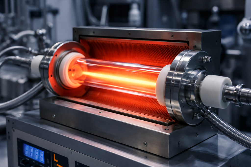
One of the most recognizable semiconductor applications is the high-purity quartz furnace tube.
Quartz process tubes can be used in high-temperature operations including:
- Oxidation
- Diffusion
- Annealing
- Thermal treatment
- Selected CVD processes
- Laboratory semiconductor processing
For semiconductor applications, specifying only an outside diameter and length is usually insufficient.
Important parameters may include:
Outer Diameter
The OD must match equipment installation and support structures.
Inner Diameter
Internal clearance affects wafer boats, carriers and process geometry.
Wall Thickness
Wall thickness and uniformity influence mechanical integrity and thermal behavior.
Straightness
Long quartz furnace tubes may require careful control of straightness over their entire length.
Roundness and Concentricity
These can become important for equipment compatibility and stable thermal processing.
End Structure
Open ends, closed ends, flanges, necks, ports and other structures may be customized according to the furnace design.
The continued construction of new semiconductor fabs creates opportunities not only for original equipment installations but also for replacement and customized quartz components used throughout the operating life of the fab.
Quartz Wafer Boats and Carriers
Quartz wafer boats are another important group of process components.
During semiconductor thermal processing, wafers need to be held at controlled spacing and orientation.
For 300mm semiconductor manufacturing, geometric accuracy becomes particularly important.
Specifications can include:
- Wafer diameter
- Slot width
- Slot pitch
- Number of wafer positions
- Boat length
- Straightness
- Dimensional tolerance
- Surface condition
- Cleaning requirements
As advanced DRAM technologies continue migrating to smaller feature sizes and more complex structures, contamination and process consistency remain critical.
A quartz boat therefore needs to provide more than mechanical support.
Material purity, dimensional repeatability and surface condition all need to be controlled.
Quartz Liners, Rings and Process Chambers
Modern semiconductor equipment also uses many quartz components that are less visible than furnace tubes.
Depending on the tool architecture, quartz parts may include:
- Quartz liners
- Quartz rings
- Quartz sleeves
- Quartz chambers
- Quartz bell jars
- Quartz shields
- Quartz plates
- Quartz discs
- Quartz flanges
- Quartz windows
- Quartz injectors
- Gas distribution components
- Precision-drilled quartz parts
Many of these components are highly customized.
Rather than purchasing a standard catalog item, semiconductor equipment manufacturers may provide technical drawings specifying dimensions, hole positions, wall thicknesses, tolerances and surface requirements.
This is why custom quartz fabrication is becoming increasingly important within the semiconductor equipment supply chain.
Semiconductor Quartz Is Moving Beyond Standard Tubes
Historically, buyers searching for quartz components might have focused mainly on quartz tubes or plates.
Today, semiconductor equipment increasingly requires more complex geometries.
A custom component may include:
multiple precision holes,
machined grooves,
welded ports,
special flanges,
concentric tube structures,
closed-end chambers,
or integrated quartz assemblies.
Manufacturing these parts requires several capabilities working together.
Precision Cutting
Quartz blanks must be cut accurately while minimizing edge damage.
Grinding and CNC Machining
Grinding and precision machining are used for dimensional control and the production of slots, holes and complex structures.
Drilling
Semiconductor equipment components may require multiple holes with controlled diameter, position and spacing.
Polishing
Depending on the application, surfaces may require mechanical polishing, optical polishing or other finishing methods.
Quartz Welding
Complex assemblies can require tubes, flanges, nozzles or ports to be fused together.
Cleaning
After fabrication, semiconductor quartz parts may require controlled cleaning to reduce particles and residues.
Inspection
Dimensional measurements, visual inspection and surface-quality checks help ensure the finished component matches customer specifications.
Purity Requirements Are Becoming More Important
High-purity fused quartz is especially valuable in semiconductor manufacturing because unwanted impurities can influence process performance.
Depending on the manufacturing environment, customers may consider parameters such as:
- Aluminum
- Iron
- Sodium
- Potassium
- Lithium
- Calcium
- Titanium
- OH content
The required purity level depends on the equipment and process.
Not every semiconductor quartz component requires the same material grade.
For example, an optical quartz window may have different material requirements from a high-temperature diffusion tube.
Similarly, a laboratory furnace tube may not require exactly the same contamination specification as a component installed in a high-volume advanced-memory fab.
Selecting the correct quartz grade should therefore begin with the actual process environment rather than simply choosing the highest specification available.
Dimensional Control Matters Alongside Material Purity
Material purity is only one component of semiconductor quartz quality.
A highly pure material can still perform poorly if the finished component has incorrect geometry.
For custom semiconductor quartz parts, customers may specify:
- OD and ID tolerances
- Wall thickness
- Flatness
- Parallelism
- Perpendicularity
- Hole diameter
- Hole position
- Concentricity
- Straightness
- Surface roughness
- Edge condition
These requirements become especially important when a quartz component must fit directly into an existing piece of semiconductor equipment.
For replacement parts, dimensional compatibility may determine whether the component can be installed without redesigning the surrounding hardware.
Global Fab Expansion Creates a Larger Installed Equipment Base
The wider industry trend extends beyond memory.
SEMI reported in October 2026 that 20 new 300mm fabs or production lines are expected to begin construction worldwide during 2026, excluding pure R&D fabs, with another 18 expected to begin construction in 2027.
The organization also projects that 13 new 300mm fabs or lines will begin operation or ship first silicon during 2026, rising to 23 in 2027.
Meanwhile, worldwide 300mm installed capacity is projected to increase around 7% in 2026, followed by approximately 8% annual growth from 2027 through 2029.
For process-component suppliers, installed capacity is an important indicator.
A semiconductor fab continues consuming spare parts, replacement components and maintenance materials long after the initial equipment is installed.
This creates potential demand across several stages:
New Equipment → Fab Qualification → Mass Production → Maintenance → Replacement → Capacity Expansion
For quartz manufacturers, this means semiconductor growth should not be viewed only as a one-time equipment purchasing cycle.
It creates a larger long-term installed base of process equipment requiring qualified components.
AI Is Raising Expectations Across the Semiconductor Supply Chain
The AI semiconductor boom is also changing what customers expect from component suppliers.
In the past, providing a quartz tube of approximately the correct dimensions might have been enough for many industrial applications.
Semiconductor customers increasingly expect more.
Typical requirements may include:
- Defined quartz material grade
- Controlled dimensional tolerances
- Technical drawings
- Inspection reports
- Consistent batch quality
- Surface-quality requirements
- Semiconductor cleaning
- Appropriate packaging
- Prototype manufacturing
- Small-batch customization
- Repeat production
For equipment manufacturers, consistency between the first prototype and later production batches can be particularly important.
The supplier therefore needs both fabrication capability and process control.
Custom Quartz Components for Semiconductor Equipment
Fuyao Quartz supplies and fabricates fused quartz components according to customer drawings, equipment requirements and application conditions.
Available product categories can include:
High-Purity Quartz Tubes
For semiconductor thermal processing, furnaces and custom equipment.
Quartz Furnace and Diffusion Tubes
Available with customized OD, ID, wall thickness, length and end structures.
Quartz Wafer Boats and Carriers
For wafer loading and high-temperature processing applications.
Quartz Plates and Discs
Available with custom dimensions, holes and surface finishing.
Quartz Rings and Flanges
Manufactured according to equipment drawings and dimensional requirements.
Quartz Windows
For observation, optical and process-equipment applications.
Custom Machined Quartz Parts
Including drilled, ground, polished and special-shaped quartz components.
Welded Quartz Assemblies
For components requiring ports, nozzles, flanges or integrated quartz structures.
For customized projects, buyers can provide drawings, samples or basic technical parameters for feasibility evaluation.
Outlook: HBM Growth Is Becoming a Manufacturing Story
AI initially appeared to be primarily a story about GPUs and advanced processors.
In 2026, it has increasingly become a semiconductor manufacturing capacity story.
HBM4 is moving into volume production.
Major memory companies are investing billions of dollars in new fabs and production infrastructure.
Global 300mm equipment spending is reaching record levels.
Memory manufacturers are expanding DRAM capacity while simultaneously migrating toward more advanced process technologies.
For the high-purity quartz supply chain, this does not mean every HBM chip directly creates demand for a specific quartz component.
The relationship is broader.
AI increases demand for advanced memory.
Advanced memory increases investment in wafer fabrication.
Additional fabs and equipment create a larger installed base of semiconductor process tools.
Those tools require high-purity, dimensionally controlled and periodically replaceable process components.
This is where high-purity fused quartz remains important.
As AI infrastructure and HBM production continue to grow, semiconductor quartz suppliers will increasingly be expected to provide not just standard material, but high-purity, precision-fabricated and application-specific process components.
For semiconductor equipment manufacturers and fabs, early communication about material grade, dimensions, tolerances, surface condition, cleaning requirements and operating environment can significantly improve the development and qualification of customized quartz parts.
The next semiconductor expansion cycle is already underway—and high-purity quartz remains one of the supporting materials behind the equipment that makes advanced chips possible.