Artificial intelligence is changing not only semiconductor chip design but also the materials used to package those chips.
Modern AI accelerators increasingly combine large logic dies, chiplets, high-bandwidth memory (HBM), high-density redistribution layers and, in some architectures, optical interconnects. As package sizes and interconnect densities increase, conventional packaging materials face growing challenges involving:
- package warpage;
- dimensional stability;
- interconnect density;
- signal loss;
- thermal expansion mismatch;
- fine-pitch routing;
- wafer thinning;
- and large-area processing.
This is one reason glass is attracting increasing attention in advanced semiconductor packaging.
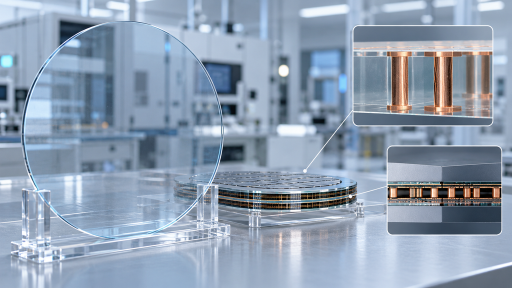
Glass is already used as a temporary carrier wafer in semiconductor manufacturing. At the same time, Through-Glass Via (TGV) technology is creating new possibilities for glass interposers and glass core substrates.
Meanwhile, hybrid bonding is pushing surface flatness, cleanliness and dimensional control to levels that increasingly resemble front-end semiconductor processing.
These technologies are developing in parallel as the semiconductor industry searches for new ways to scale AI systems.
The direction became particularly visible in October 2026, when Applied Materials and Besi announced an expanded partnership targeting next-generation packaging for AI, including new hybrid bonding platforms, thermo-compression bonding, die-on-wafer, die-on-die and die-on-panel integration.
So why is glass becoming increasingly important?
The answer begins with understanding the different roles glass can play.
Glass Does Not Have Only One Role in Advanced Packaging
When discussing glass in semiconductor packaging, it is important to distinguish between several applications.
1. Glass Carrier Wafer
A glass carrier temporarily supports another wafer or reconstructed package during processes such as:
- wafer thinning;
- backside grinding;
- polishing;
- temporary bonding;
- fan-out wafer-level packaging;
- redistribution layer processing;
- and some advanced 2.5D/3D integration flows.
The carrier is normally removed later.
2. Glass Interposer or TGV Substrate
In this application, the glass itself becomes part of the electrical package.
Through-Glass Vias are formed through the substrate and metallized to provide vertical electrical connections.
3. Glass Core Substrate
Glass can also act as the structural core of an advanced IC substrate, potentially replacing or supplementing traditional organic core materials.
4. Glass in Hybrid-Bonding Process Flows
Glass is not inherently required for hybrid bonding.
However, high-flatness glass carriers can support thin wafers, reconstructed wafers or other structures during process steps associated with advanced bonding.
These distinctions are important because the material specifications for each application can be very different.
Why AI Packaging Is Putting More Pressure on Conventional Materials
Traditional semiconductor packages were relatively small.
AI packages are moving in the opposite direction.
A high-performance AI package may integrate:
GPU / AI accelerator + HBM + chiplets + interposer + substrate + high-density RDL
into a very large package.
As package dimensions increase, material deformation becomes harder to control.
Different materials expand at different rates when heated.
This behavior is described by the Coefficient of Thermal Expansion, or CTE.
When silicon, copper, molding compound, organic substrate and other materials are assembled together, differences in CTE can generate mechanical stress.
The result may include:
- Bow;
- Warp;
- delamination;
- RDL deformation;
- alignment errors;
- solder-joint stress;
- and lower manufacturing yield.
Glass offers manufacturers another way to manage this problem because its composition can be engineered to provide specific thermal and mechanical properties.
Corning, for example, currently offers semiconductor glass carriers across multiple CTE ranges and states that its advanced packaging carriers can reduce in-process warp by up to 40% in certain processes.
This does not mean glass eliminates warpage.
It means glass provides another material-engineering variable that packaging engineers can optimize.
1. Glass Carrier Wafers: Supporting Thin and Fragile Structures
One of the most mature semiconductor applications for glass is the temporary carrier wafer.
Modern device wafers are often thinned substantially during packaging.
A silicon wafer may begin relatively thick but later undergo backside grinding and polishing to reduce thickness.
Once thin, the wafer becomes mechanically fragile.
It can:
- bend;
- crack;
- warp;
- break during handling;
- or lose dimensional stability during thermal processing.
A temporary carrier helps stabilize the wafer.
A simplified process can be represented as:
Device Wafer → Temporary Bonding → Glass Carrier → Wafer Thinning / Processing → Debonding
Glass is particularly attractive for this application for several reasons.
Low TTV
Total Thickness Variation is one of the most important specifications for carrier wafers.
A carrier with poor TTV may transfer geometry errors into the bonded stack.
Low TTV improves process stability during:
- grinding;
- lithography;
- bonding;
- coating;
- CMP;
- and metrology.
For advanced applications, average thickness alone is therefore insufficient.
Engineers must also consider the variation across the complete wafer.
Flatness and Warp
A highly warped carrier can make precision processing difficult.
This becomes particularly important as:
- wafer diameter increases;
- package dimensions increase;
- RDL pitch decreases;
- and bonding alignment becomes tighter.
Ultra-flat glass can help maintain the geometry of the temporary bonded stack.
Tunable CTE
Different packaging structures may require different carrier CTE values.
One advantage of engineered glass is that the composition can be adjusted to provide a range of thermal-expansion characteristics.
The carrier can therefore be selected according to the materials in the process stack rather than treating all carrier wafers as identical.
Optical Transparency
This is another significant advantage.
Because many glass materials are transparent at selected wavelengths, laser-based temporary bonding or debonding processes may operate through the carrier.
This can be particularly useful for advanced wafer handling.
Corning specifically identifies transparency, low warp, low TTV and adjustable CTE as important benefits of semiconductor glass carriers.
2. From Carrier Wafer to Permanent Glass Substrate
The more disruptive opportunity is when glass moves from being a temporary process tool to becoming part of the package itself.
This is where Through-Glass Via technology becomes important.
A TGV is a microscopic opening passing through a glass substrate.
The via can then be metallized to create an electrical pathway from one side of the glass to the other.
The concept resembles Through-Silicon Via technology, but the material properties and manufacturing processes are different.
A simplified TGV process may include:
- glass material selection;
- TGV hole formation;
- cleaning;
- sidewall conditioning;
- seed/barrier layer deposition;
- copper metallization;
- via filling or conformal plating;
- planarization;
- RDL formation;
- inspection.
The exact sequence depends heavily on the substrate design and TGV architecture.
Why TGV Is Attractive for AI Packaging
AI processors require enormous amounts of data to move rapidly between:
- logic;
- HBM;
- chiplets;
- accelerators;
- networking devices;
- and optical interfaces.
The interconnection structure therefore becomes almost as important as the transistor architecture.
Glass has several potentially useful electrical properties.
It is an electrical insulator and can exhibit low dielectric loss, making it attractive for high-frequency signal transmission.
TGVs allow signals and power to travel vertically through the substrate.
This creates opportunities for:
- 2.5D packaging;
- RF packaging;
- chiplet integration;
- high-density RDL;
- co-packaged optics;
- photonics;
- and AI accelerator packages.
Glass can also be produced in wafer and large-panel formats, opening a possible path toward larger packaging areas.
TGV Manufacturing Is Still One of the Major Challenges
The concept of TGV is straightforward.
Producing millions of reliable microscopic vias economically is much more difficult.
Several manufacturing methods are being developed.
These include:
- laser drilling;
- laser modification followed by chemical etching;
- wet etching;
- photosensitive glass processing;
- and combinations of laser and chemical processes.
Each approach creates different trade-offs involving:
via diameter, aspect ratio, taper, sidewall roughness, throughput and cost.
Via Diameter
Smaller vias enable higher interconnection density.
However, decreasing via diameter makes metallization and complete copper filling more difficult.
Aspect Ratio
Aspect ratio is approximately:
Glass Thickness ÷ Via Diameter
For example, a thick glass substrate combined with a very small via can create a high-aspect-ratio structure.
Such structures are difficult to etch, coat and fill uniformly.
Sidewall Quality
Poor TGV sidewall quality can create:
- microcracks;
- stress concentration;
- metallization discontinuity;
- electrical reliability problems;
- and reduced mechanical strength.
Copper-to-Glass Adhesion
Glass and copper have very different material properties.
Achieving reliable adhesion between the glass surface, barrier/seed layers and copper metallization is therefore a major process challenge.
Copper Filling
Incomplete filling may produce:
- voids;
- seams;
- resistance variation;
- reliability failures.
For this reason, TGV manufacturing cannot be evaluated by hole diameter alone.
A technically meaningful TGV specification should consider the complete via structure.
Important TGV Parameters
For engineers evaluating a TGV glass substrate, useful parameters may include:
| Parameter | Why It Matters |
|---|---|
| Glass thickness | Determines mechanical structure and via aspect ratio |
| TGV diameter | Determines interconnection density |
| TGV pitch | Controls routing density |
| Via taper | Affects metallization and design |
| Aspect ratio | Influences etching and filling difficulty |
| Position tolerance | Critical for lithography and assembly |
| Sidewall roughness | Influences metallization and reliability |
| Microcracks | Affect mechanical strength |
| Copper fill quality | Determines electrical reliability |
| TTV | Affects downstream processing |
| Bow / Warp | Influences lithography and assembly |
| Surface roughness | Important for RDL and bonding |
| CTE | Influences package stress |
In July 2026, reports around TGV development highlighted continuing work on thicker glass structures, metallization, micro-defect reduction and warpage control, illustrating that industrial development is now moving beyond simply demonstrating holes in glass toward solving production-yield issues.
3. Glass Core Substrates: Why the Industry Is Interested
Organic substrates have supported semiconductor packaging for decades.
They remain essential and will continue to dominate many applications.
However, advanced AI packages are pushing toward:
- larger package dimensions;
- finer wiring;
- more I/O connections;
- greater dimensional stability;
- and higher signal frequencies.
Glass is being investigated as a potential core material because it can provide:
- high dimensional stability;
- low surface roughness;
- tunable CTE;
- potentially fine wiring;
- favorable high-frequency electrical properties;
- and compatibility with larger panel formats.
TrendForce reported in June 2026 that the rapid expansion of AI semiconductors is accelerating development of panel-level packaging. It identified 2026 as an important validation period for related equipment and materials, while also noting that glass-core-substrate commercialization still faces substantial technical challenges.
This distinction is important.
Glass core substrates are promising, but they should not yet be described as having universally replaced organic substrates.
The industry is still working through manufacturing, yield and cost challenges.
4. Why Glass and Hybrid Bonding Are Often Discussed Together
Hybrid bonding is another major technology being developed for AI and high-performance computing.
It enables extremely dense connections between:
- wafer and wafer;
- die and wafer;
- or potentially other advanced integration structures.
Unlike conventional solder-bump connections, hybrid bonding can combine direct dielectric bonding with very fine copper-to-copper interconnects.
This can reduce interconnect dimensions and create much shorter electrical paths.
The potential advantages include:
- higher interconnect density;
- higher bandwidth;
- lower electrical parasitics;
- improved power efficiency;
- and tighter 3D integration.
However, hybrid bonding places exceptionally strict requirements on the surfaces being joined.
Critical parameters include:
- surface flatness;
- CMP quality;
- Cu recess or protrusion;
- surface roughness;
- particle contamination;
- alignment accuracy;
- wafer Bow and Warp;
- and surface preparation.
Applied Materials and Besi’s October 1, 2026 announcement illustrates how strategically important the technology has become. Their expanded collaboration now covers hybrid bonding as well as TCB, die-on-wafer, die-on-die, die-on-panel and photonics integration for AI systems.
Does Hybrid Bonding Require a Glass Wafer?
No.
This is an important distinction.
Hybrid bonding can be performed without glass.
Glass becomes relevant because advanced packaging frequently requires temporary support, wafer thinning and extremely precise control of geometry before bonding.
For example, a thin wafer may be temporarily bonded to an ultra-flat glass carrier while undergoing:
- thinning;
- backside processing;
- RDL processing;
- surface preparation;
- or other manufacturing steps.
The carrier helps preserve wafer geometry.
It may then be removed before the final hybrid-bonding step.
In other architectures, TGV glass or glass core substrates may be part of the package itself.
Therefore, the relationship can be summarized as:
Hybrid Bonding ≠ Glass
but
Advanced Hybrid-Bonding Process Flows → Increasing Need for Precise Carrier and Substrate Engineering
This is one reason ultra-low-TTV carrier wafers and high-flatness glass are receiving more attention.
5. From Wafer-Level to Panel-Level Packaging
One of the most interesting characteristics of glass is that it can be produced not only as circular wafers but also as large rectangular panels.
Examples of advanced packaging form factors include:
- 200 mm wafer;
- 300 mm wafer;
- 310 × 310 mm panel;
- 510 × 515 mm-class panel;
- and other customized large formats.
Larger panel formats could theoretically increase the number of packages processed simultaneously.
This creates potential manufacturing-economics advantages.
But scaling the panel introduces another set of challenges.
Large-area glass must maintain:
- thickness uniformity;
- dimensional stability;
- low warp;
- accurate TGV positioning;
- consistent metallization;
- uniform RDL;
- and mechanical strength across the complete panel.
Therefore:
larger panel ≠ automatically lower cost.
The benefit only appears if the process yield remains sufficiently high.
This is particularly important for AI packages because individual package sizes are becoming very large.
6. Glass vs Silicon vs Organic Packaging Materials
There is unlikely to be one universal substrate material for every semiconductor package.
Each material has advantages.
| Property | Glass | Silicon | Organic |
|---|---|---|---|
| Dimensional stability | High | Very High | Moderate |
| Electrical insulation | Excellent | Requires isolation | Excellent |
| High-frequency loss | Potentially Low | Application dependent | Material dependent |
| TGV / TSV capability | TGV | TSV | Mechanical / laser vias |
| CTE tunability | Good | Limited | Formulation dependent |
| Large-panel scalability | Strong potential | Limited | Established |
| Fine routing potential | High | Very High | Improving |
| Processing maturity | Developing | High | Very High |
| Cost maturity | Developing | Expensive for large areas | Established |
The future is therefore more likely to involve heterogeneous materials than one material replacing every other material.
Silicon may remain advantageous where extremely dense interconnection is required.
Organic substrates may continue to dominate applications where cost and established manufacturing infrastructure are critical.
Glass may occupy an increasingly important space where:
large area + dimensional stability + fine routing + TGV + electrical performance
need to be combined.
7. What Engineers Should Specify for Glass Carrier Wafers
When sourcing carrier glass for semiconductor processing, simply requesting a:
“300 mm glass wafer”
is normally insufficient.
A more complete specification should consider:
Dimensions
- diameter;
- thickness;
- thickness tolerance;
- edge profile.
Geometry
- TTV;
- Bow;
- Warp;
- flatness.
Surface
- surface roughness;
- scratch-dig or cosmetic criteria where relevant;
- surface particles;
- edge chips.
Material
- glass composition;
- CTE;
- Young’s modulus;
- thermal resistance;
- optical transmission.
Process Compatibility
- bonding method;
- debond method;
- process temperature;
- chemical compatibility;
- vacuum chuck compatibility.
These parameters should be determined according to the actual packaging process rather than selecting a carrier based on diameter alone.
8. What Engineers Should Specify for TGV Glass
TGV substrates require an additional set of specifications.
A practical request should define:
Glass
- material type;
- diameter or panel dimensions;
- thickness;
- TTV;
- Bow;
- Warp.
TGV
- via diameter;
- pitch;
- number of vias;
- via shape;
- taper;
- positional accuracy;
- aspect ratio.
Metallization
- Cu thickness;
- filled or conformal structure;
- seed layer;
- barrier layer;
- via resistance if required.
Surface
- Ra;
- RDL requirement;
- planarization;
- metallization surface condition.
Inspection
- microcracks;
- incomplete vias;
- voids;
- metallization defects;
- via-position map.
As TGV dimensions become smaller, the relationship between these specifications becomes increasingly important.
The Real Opportunity Is Materials Integration
The rise of glass in AI packaging should not be interpreted as a simple story of:
“glass replacing silicon.”
The more important trend is the increasing importance of materials integration.
AI chips are forcing the industry to optimize the entire stack:
Logic → HBM → Chiplets → Interposer → RDL → Core Substrate → Carrier → Bonding Interface
Each layer affects the others.
A carrier with excessive warp can affect lithography.
Poor TGV geometry can affect metallization.
Poor surface flatness can affect bonding.
CTE mismatch can affect package reliability.
Particle contamination can destroy a hybrid bond.
This is why advanced packaging is increasingly beginning to resemble front-end semiconductor manufacturing.
Applied Materials described this shift directly in its October 2026 announcement, emphasizing that next-generation packaging now requires materials engineering, precision processing, metrology, inspection and particle control comparable to disciplines traditionally associated with wafer fabrication.
From Glass Carrier to TGV and Hybrid Bonding
Glass is becoming strategically important because it can serve several very different functions across the advanced packaging process.
As a carrier wafer, it can provide temporary mechanical support and dimensional stability.
As a TGV substrate or interposer, it can provide high-density vertical electrical connections.
As a glass core substrate, it offers a possible platform for large, fine-pitch packages.
And within hybrid-bonding process flows, ultra-flat carriers can help maintain the precision required for increasingly thin and complex structures.
The industry still has major challenges to solve, especially in:
- TGV yield;
- copper adhesion;
- via metallization;
- microcrack control;
- panel warpage;
- large-area RDL;
- bonding cleanliness;
- process throughput;
- and overall manufacturing cost.
But the direction is becoming increasingly clear.
As AI systems demand larger packages, higher bandwidth and denser chip-to-chip connections, packaging materials can no longer be treated as passive mechanical supports.
They are becoming part of semiconductor performance itself.
And that is why glass carrier wafers, TGV substrates and precision glass materials are becoming increasingly important components of the AI advanced-packaging roadmap.