Wafer dicing may appear to be one of the simplest steps in semiconductor manufacturing: cut a processed wafer into individual dies.
In reality, it has become increasingly difficult.
Modern semiconductor wafers are becoming thinner, harder, more brittle and more valuable. At the same time, advanced packaging requires smaller dicing streets, higher die strength and tighter control of chipping, cracks and contamination.
Materials such as silicon carbide, sapphire, GaAs, GaN and glass introduce additional challenges that conventional silicon dicing processes were not originally designed to solve.
This is why wafer singulation in 2026 is no longer dominated by one technology.
Manufacturers can now choose between blade dicing, conventional laser dicing, Stealth Dicing and ultrashort-pulse technologies such as femtosecond laser dicing.
The correct choice depends on the wafer material, thickness, device structure, street width, acceptable heat-affected zone, throughput and cost.
Recent equipment developments illustrate this shift. In September 2026, ASMPT announced that its new ALSI LASER1206 platform would be presented for high-precision wafer dicing and grooving in advanced memory, logic, AI and power applications. Its multi-beam UV laser approach is designed to minimize thermal impact while reducing burr formation and preserving die strength.
Earlier in February 2026, TRUMPF and LIDROTEC announced a laser dicing process designed for semiconductor mass production that they said could achieve cutting speeds more than three times those of conventional mechanical sawing while maintaining high edge quality.
The direction is clear:
Wafer dicing is moving from simple mechanical separation toward increasingly material-specific precision engineering.
Why Dicing Quality Matters
The purpose of wafer dicing is not merely to separate dies.
A high-quality dicing process must preserve the mechanical and electrical integrity of every die near the cut line.
Poor dicing can create:
chipping, microcracks, delamination, particle contamination, thermal damage, metal burrs, low die strength and excessive kerf loss.
These defects are particularly important for thin dies and brittle semiconductor materials.
A small crack generated during dicing may not immediately break a chip. However, subsequent die attach, thermal cycling or packaging stress can cause the crack to propagate.
For this reason, the quality of the diced edge increasingly affects downstream package reliability.
1. Blade Dicing: The Established Industry Standard
Blade dicing remains one of the most widely used wafer singulation technologies.
The principle is straightforward.
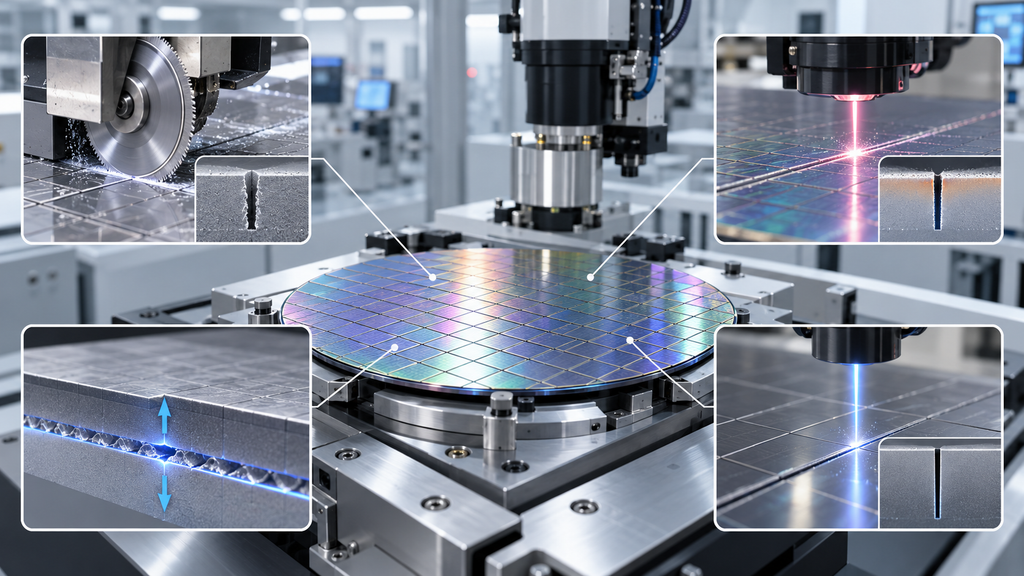
A high-speed spindle rotates a thin diamond-containing dicing blade while the wafer is moved beneath it along predefined streets.
The blade mechanically removes material until the wafer is completely separated.
Despite the development of multiple laser alternatives, blade dicing remains attractive because it is mature, predictable and relatively cost-effective.
DISCO continues to develop specialized blade technologies for silicon, compound semiconductors, oxides, ceramics and other brittle materials. Its current blade portfolio illustrates how grit size, blade rigidity and diamond concentration are optimized according to chipping, blade life and material characteristics.
Advantages of Blade Dicing
The strongest advantage is manufacturing maturity.
There is a very large installed base of dicing saws, extensive process knowledge and a wide selection of blades.
Blade dicing can also process many materials, including silicon, sapphire, ceramics, compound semiconductor wafers and glass.
For conventional silicon wafers with sufficient street width and moderate thickness, it can still offer an excellent balance between cost and productivity.
Main Limitation: Mechanical Stress
The blade physically contacts the wafer.
This creates mechanical load at the cut edge.
For brittle materials, mechanical forces may generate surface or backside chipping.
This becomes especially important as wafer thickness decreases.
DISCO notes that backside chipping becomes more difficult to control when processing very thin wafers, and finer-grit blades are often required to reduce the mechanical shock introduced during cutting.
The challenge becomes even greater for hard or brittle materials such as:
SiC, sapphire, GaAs and certain ceramic substrates.
Feed speed, blade grit, blade thickness, spindle speed and crystal orientation can all influence edge quality.
Kerf Width and Material Loss
Blade dicing physically removes material.
The width removed by the blade is known as the kerf.
This means the design must provide a sufficiently wide dicing street.
For expensive semiconductor materials, kerf loss matters economically.
This is particularly significant for materials such as SiC, where crystal growth and wafer production are comparatively expensive.
Reducing the dicing street can potentially allow more dies to be obtained from each wafer.
This is one reason laser and Stealth Dicing technologies are attracting greater interest.
2. Laser Ablation Dicing: Non-Contact Cutting
Laser dicing eliminates the mechanical blade.
Instead, focused laser energy removes wafer material.
In conventional laser ablation dicing, the laser is focused on or near the wafer surface.
The energy causes localized material removal through processes involving melting, vaporization or ablation, depending on wavelength, pulse duration and material.
Because there is no rotating blade contacting the wafer, mechanical stress can be reduced substantially.
This makes laser dicing attractive for brittle and thin semiconductor materials.
DISCO reports that laser full-cut processes can provide narrower kerfs and higher feed speeds for certain compound semiconductor applications. In one GaAs example, it reports significantly higher processing speed than conventional blade cutting, although actual performance depends on the wafer and process.
Main Advantages
Laser dicing can provide narrow streets, flexible cut geometries and non-contact processing.
It can also be used where mechanical blades struggle with complicated multilayer structures.
Another important application is laser grooving followed by blade dicing.
This hybrid approach can remove difficult top layers such as low-k dielectric structures before the mechanical blade performs the deeper cut.
The objective is to prevent peeling or uncontrolled cracking in sensitive surface films.
The Main Laser Problem: Heat-Affected Zone
Although conventional laser cutting eliminates mechanical contact, it introduces another problem:
heat.
When laser energy is absorbed by the wafer, the surrounding region may experience thermal modification.
This can produce:
recast material, molten residue, microcracks, oxidation, discoloration or reduced die strength.
DISCO’s January 2026 review of GaAs dicing notes that although laser ablation can suppress chipping compared with blade dicing, thermal damage may reduce chip flexural strength if the process is not properly controlled.
The industry therefore continues to improve:
laser wavelength, pulse duration, beam shape, scanning strategy and debris removal.
ASMPT’s current multi-beam UV development is an example of this trend toward reducing thermal effects during dicing.
3. Stealth Dicing: Modify the Wafer from the Inside
Stealth Dicing is fundamentally different from surface laser ablation.
Instead of removing material from the surface, a laser is focused inside the wafer.
The laser creates a modified layer within the material along the intended dicing line.
The wafer is subsequently expanded, and the dies separate along the weakened internal region.
Hamamatsu Photonics describes the process as two principal steps: laser irradiation creates an internal modified layer and cracks, followed by an expansion process that separates the wafer.
This means conventional surface kerf removal can be greatly reduced.
DISCO, an alliance partner for the technology, highlights three particularly important characteristics: dry processing, reduced contamination and very narrow streets.
Why Stealth Dicing Is Attractive for Brittle Wafers
Because cutting occurs through internal modification rather than mechanically grinding material away, Stealth Dicing can significantly reduce surface chipping.
This makes it attractive for materials including:
silicon, sapphire, SiC, GaAs and other crystalline substrates, depending on material optical characteristics and process configuration.
DISCO currently lists sapphire, SiC and GaAs among materials that can be processed using suitable laser configurations.
Another important advantage is that the process can be completely dry.
This matters for MEMS devices containing cavities, membranes or sensitive structures that may be damaged by dicing water.
Hamamatsu specifically identifies MEMS and memory applications as areas where the technology can offer advantages such as dry processing, reduced kerf loss and improved die strength.
Stealth Dicing Before Grinding
A particularly interesting variation is SDBG — Stealth Dicing Before Grinding.
Here, the internal modification is created before the wafer reaches its final thickness.
The wafer is then ground thinner.
Hamamatsu identifies SDBG as a process suitable for ultra-thin semiconductor devices below approximately 50 µm thickness, where maintaining mechanical strength becomes especially important.
This is relevant to:
memory stacking, 3D packaging, ultra-thin ICs and other advanced packaging applications.
As chip thickness continues to decrease, dicing and thinning increasingly need to be designed together rather than as independent processes.
4. Femtosecond Laser Dicing: Reducing Thermal Interaction
Femtosecond laser processing belongs to the broader category of ultrashort-pulse laser processing.
One femtosecond is:
10⁻¹⁵ seconds.
The extremely short pulse duration allows a large amount of energy to be deposited into a very small area before significant heat can diffuse into the surrounding material.
This fundamentally changes the interaction between the laser and wafer compared with longer-pulse laser processes.
In well-optimized applications, this can reduce:
heat-affected zones, recast layers, thermal cracking and unwanted material modification.
For this reason, ultrashort-pulse laser processing is increasingly attractive for high-value brittle materials.
Coherent, for example, currently identifies high-power ultrashort-pulse lasers as suitable for semiconductor wafer dicing and specifically cites sapphire wafer dicing as an application.
Why Femtosecond Lasers Matter for Sapphire and SiC
Sapphire and SiC are particularly difficult materials to process.
Both are hard and brittle.
Mechanical cutting can generate chipping and microcracks.
Conventional thermal laser processing can introduce heat-related damage.
Ultrashort-pulse processing offers a middle path:
non-contact cutting with substantially reduced thermal diffusion.
For sapphire, this is particularly relevant to LED and optical-device manufacturing.
For SiC, femtosecond and other ultrashort-pulse techniques are attractive because of the material’s extreme hardness and increasing value as wafer diameter grows from 150 mm toward 200 mm.
However, femtosecond processing should not be described as automatically superior.
The actual result depends on:
pulse energy, wavelength, repetition rate, focus position, scan strategy, wafer thickness and material structure.
Femtosecond Dicing vs Conventional Laser Dicing
The basic difference is the timescale of energy deposition.
Longer-pulse laser processes allow more heat to spread into surrounding material.
Ultrashort pulses localize the energy more strongly.
In practice, this often means femtosecond processing can produce a smaller heat-affected zone.
But there are trade-offs.
Femtosecond laser systems are more complex and expensive.
Throughput can also become a challenge if a process requires many passes or large volumes of material to be removed.
Consequently, femtosecond technology is most attractive where edge quality and damage control are worth more than the lowest possible equipment cost.
Blade vs Laser vs Stealth vs Femtosecond
| Parameter | Blade Dicing | Laser Ablation | Stealth Dicing | Femtosecond Dicing |
|---|---|---|---|---|
| Cutting Principle | Mechanical removal | Surface laser ablation | Internal laser modification + separation | Ultrashort-pulse material removal/modification |
| Physical Contact | Yes | No | No | No |
| Water Required | Usually | Process dependent | No | Process dependent |
| Mechanical Stress | Higher | Low | Very Low | Very Low |
| Thermal Effect | Very Low | Moderate, process dependent | Low at surfaces | Very Low when optimized |
| Kerf Width | Relatively wider | Narrow | Very narrow | Narrow |
| Surface Chipping | Possible | Low | Very low | Very low |
| Debris | Blade particles/slurry | Possible ablation debris | Very low | Usually lower than conventional ablation |
| Complex Shapes | Limited | Good | Mostly separation paths | Excellent |
| Thin Wafer Suitability | Challenging | Good | Excellent | Excellent |
| Typical Strength | Cost and maturity | Speed and flexibility | Minimal kerf and dry process | High precision and minimal thermal damage |
| Main Challenge | Chipping/blade wear | HAZ and debris | Material/process limitations | Cost and throughput |
This table should be used only as a general comparison.
Actual performance can change significantly according to wafer material, device layer structure, thickness and equipment configuration.
Which Dicing Method Is Best for Silicon?
For conventional silicon wafers, blade dicing remains highly competitive.
It is mature, economical and well understood.
However, laser technology becomes more attractive when wafers are very thin, street width becomes limited or the surface contains difficult dielectric structures.
Stealth Dicing can also be attractive for thin silicon devices and SDBG applications.
Therefore, there is no universal reason to replace mechanical dicing for standard silicon production.
Which Method Is Best for SiC?
SiC is much more difficult.
Its hardness increases blade wear and makes cutting more demanding.
Chipping and microcracks must also be controlled carefully because the wafer and individual dies are valuable.
Blade dicing can still be used when the correct blade and process parameters are selected.
However, laser and Stealth Dicing become increasingly attractive when the priority is:
narrow streets, low chipping and high die strength.
DISCO specifically identifies Stealth Dicing as capable of high-quality processing for brittle materials such as SiC and GaN without conventional blade-induced chipping.
For extremely demanding edge-quality applications, ultrashort-pulse laser processing may also become an important alternative.
Which Method Is Best for Sapphire?
Sapphire is another hard, brittle crystal.
Blade dicing is possible but requires careful control of blade specification and processing conditions.
Laser techniques are attractive because they minimize mechanical contact.
Stealth Dicing is already well established for sapphire applications, particularly in LED manufacturing.
Ultrashort-pulse laser processes are also increasingly used because they can reduce thermal and mechanical damage.
For high-quality sapphire components, however, the final decision should consider not only cutting speed but also:
edge chipping, subsurface damage, die strength and downstream polishing requirements.
Which Method Is Best for Glass?
Glass requires a somewhat different assessment.
Its transparency can make laser interaction strongly dependent on wavelength and focus strategy.
Conventional mechanical dicing is possible for many glass types.
However, ultrashort-pulse lasers are becoming particularly important for advanced glass applications because nonlinear absorption can be used to process transparent materials locally.
This is relevant for:
glass wafers, TGV substrates, optical glass and advanced packaging glass.
As advanced packaging moves toward glass carriers and glass-core technologies, laser processing of glass will become increasingly important.
2026: Wafer Dicing Is Becoming an Advanced Packaging Technology
Historically, dicing was viewed primarily as a back-end separation operation.
That is changing.
Advanced packaging integrates:
wafer thinning, temporary bonding, RDL, hybrid bonding, chiplets, HBM and ultra-thin dies.
Dicing must now fit into the complete process flow.
A poor singulation process may destroy the mechanical strength gained during wafer thinning.
Excessive particles may interfere with bonding.
Large kerf widths reduce the usable wafer area.
Thermal damage can reduce die reliability.
This explains why equipment suppliers are investing in more sophisticated laser platforms.
At SEMICON West 2026, ASMPT is positioning laser dicing alongside hybrid bonding, thermocompression bonding and advanced packaging technologies for AI and HPC.
At SEMICON Korea earlier in 2026, TRUMPF and LIDROTEC highlighted a laser process combining beam shaping and liquid-assisted debris removal, with an emphasis on both high speed and high edge quality.
These developments indicate that dicing is becoming increasingly integrated with the broader advanced-packaging roadmap.
How to Select a Wafer Dicing Process
The correct dicing method should not be selected simply by asking:
“Which technology is newest?”
The more useful question is:
“Which technology produces the required die quality at an acceptable cost and throughput for this particular wafer?”
The evaluation should consider material type, wafer diameter and thickness, dicing street width, surface layers, backside films, acceptable chipping, heat sensitivity, target die strength, contamination limits and annual production volume.
For a standard silicon wafer, a mature blade process may still be the optimal solution.
For brittle SiC or sapphire, Stealth Dicing or advanced laser processing may justify the additional equipment cost.
For heat-sensitive, high-value or extremely precise structures, femtosecond processing may provide advantages that conventional laser systems cannot achieve.
The best process is therefore not necessarily the most advanced process.
It is the process that provides the required yield, quality and economics.
The Future Is Hybrid, Not One Technology
It is unlikely that one dicing technology will replace all others.
Blade dicing continues to improve.
Laser ablation is becoming faster and more precise.
Stealth Dicing offers unique advantages for narrow streets, dry processing and thin wafers.
Femtosecond and other ultrashort-pulse technologies are pushing the limits of low-damage machining.
And some manufacturing flows already combine multiple technologies.
For example:
laser grooving + blade dicing
can combine precise surface-layer removal with efficient mechanical separation.
Similarly:
Stealth Dicing + backside grinding
creates the SDBG process for extremely thin devices.
The future of wafer singulation will therefore be determined less by a competition between “blade versus laser” and more by increasingly customized processes for specific semiconductor materials.
For silicon, SiC, sapphire, GaN, GaAs and glass, the central engineering question will remain the same:
How can the wafer be separated while preserving the maximum possible die strength, usable area and manufacturing yield?
In 2026, that question is making wafer dicing one of the more technically important steps in advanced semiconductor manufacturing.