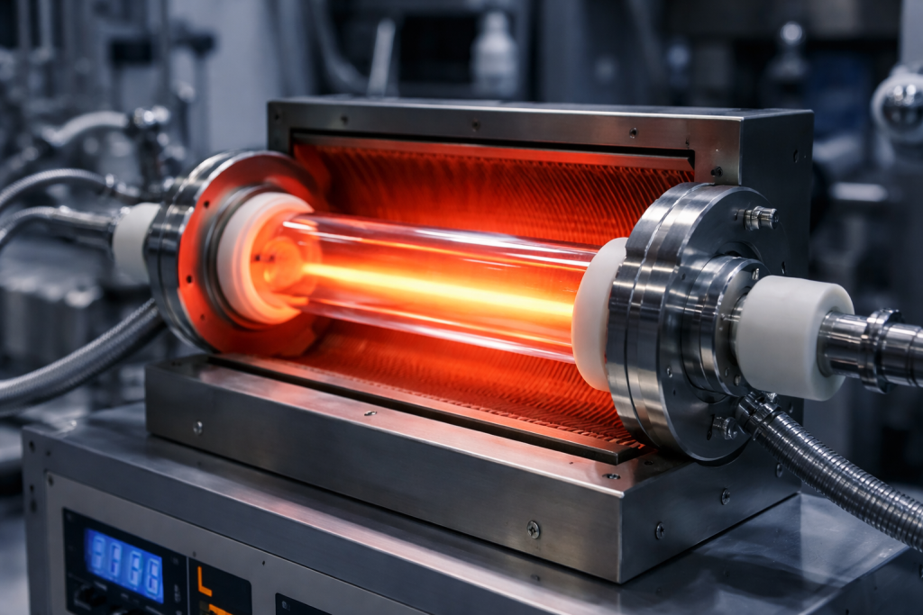
As semiconductor devices continue to evolve toward higher integration, advanced packaging, and heterogeneous system architectures, the demand for specialized substrate materials has increased significantly. Among these materials, glass wafers have emerged as an important platform for microelectronics, photonics, sensors, and advanced packaging technologies.
Traditionally, silicon wafers have dominated semiconductor manufacturing. However, стеклянные пластины offer unique optical, thermal, electrical, and chemical properties that make them valuable complementary materials in a wide range of high-tech applications. From MEMS devices and image sensors to augmented reality (AR) optics and wafer-level packaging, glass wafers are becoming increasingly important in next-generation electronic systems.
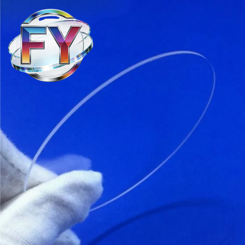
What Is a Glass Wafer?
A glass wafer is a precision-engineered circular substrate fabricated from specialized glass materials, including fused silica, quartz glass, alkali-free glass, and glass-silicon composite structures.
Unlike conventional optical glass components, glass wafers are manufactured with semiconductor-grade requirements, including:
- Ultra-low surface roughness
- Высокая точность размеров
- Tight thickness control
- Excellent flatness
- Superior optical transparency
These characteristics enable glass wafers to meet the demanding requirements of modern semiconductor and photonic manufacturing.
Key Properties of Glass Wafers
Excellent Chemical Resistance
Glass wafers exhibit strong resistance to acids, solvents, and various processing chemicals commonly used in semiconductor fabrication. This stability ensures long-term reliability during manufacturing and operation.
Превосходная термическая стабильность
Many glass materials can withstand elevated temperatures while maintaining dimensional stability. Their low coefficient of thermal expansion helps minimize thermal stress and deformation during processing.
Высокая оптическая прозрачность
Glass wafers offer excellent transmission across ultraviolet (UV), visible, and infrared (IR) wavelength ranges, depending on material composition. This makes them ideal for optical and photonic applications.
Smooth Surface Quality
Advanced polishing technologies allow glass wafers to achieve extremely low surface roughness, which is critical for precision optics, lithography, and sensor fabrication.
Electrical Insulation
Glass possesses excellent dielectric properties, including low dielectric loss and high electrical resistivity, making it suitable for high-frequency electronic applications.
Types of Quartz Glass Wafers
Quartz glass wafers are among the most widely used glass wafer materials due to their exceptional purity and thermal performance.
Synthetic UV-Grade Quartz Glass
Produced through chemical vapor deposition (CVD) processes, synthetic quartz contains a relatively high hydroxyl content and extremely low metallic impurities.
Typical characteristics include:
- Высокий уровень пропускания ультрафиолета
- Excellent radiation resistance
- High optical purity
These materials are commonly used in ultraviolet optical systems and advanced photonics applications.
Flame-Fused Optical Quartz Glass
Manufactured using hydrogen-oxygen flame fusion technology, this type of quartz offers:
- Высокая химическая чистота
- Good UV transmission
- Отличная термическая стабильность
It is widely used in semiconductor processing equipment and precision optical components.
Vacuum-Melted Infrared Quartz Glass
Produced under vacuum and high-temperature conditions, infrared quartz glass features:
- Very low hydroxyl concentration
- Excellent infrared transmission
- Reduced infrared absorption
These properties make it suitable for infrared imaging systems and laser applications.
Thermal and Electrical Characteristics
Glass wafers possess several important physical properties that contribute to their widespread use.
Тепловые свойства
Quartz-based glass materials demonstrate:
- Melting temperatures above 1700°C
- Чрезвычайно низкое тепловое расширение
- Высокая устойчивость к тепловым ударам
- Stable performance under elevated temperatures
These characteristics are critical for semiconductor manufacturing environments.
Электрические свойства
Glass wafers maintain:
- High dielectric strength
- Low dielectric loss
- Excellent insulation performance
even under high-temperature operating conditions.
Such properties support their use in advanced electronic and RF systems.
Applications of Glass Wafers
Устройства MEMS
Glass wafers are widely used in Micro-Electro-Mechanical Systems (MEMS), including:
- Датчики давления
- Accelerometers
- Gyroscopes
- Микрофлюидные устройства
Their transparency and insulating properties make them particularly attractive for MEMS packaging.
CMOS and CCD Image Sensors
Glass wafers serve as substrates and cover materials in image sensor manufacturing, helping improve optical performance and environmental protection.
Microwave and RF Electronics
Due to their low dielectric loss, glass substrates are increasingly used in:
- High-frequency circuits
- Antenna structures
- RF modules
- Communication devices
where signal integrity is critical.
Оптические компоненты
Glass wafers are extensively used in the production of:
- Оптические окна
- Prisms
- Lenses
- Laser optics
- Photonic devices
Their high optical quality enables precise light transmission and manipulation.
AR and MR Wearable Devices
The rapid development of augmented reality (AR) and mixed reality (MR) technologies has created new demand for ultra-thin, high-precision glass wafers.
Приложения включают:
- Waveguides
- Optical combiners
- Display modules
- Projection optics
Glass provides the transparency and dimensional accuracy required for immersive wearable systems.
Glass Wafers in Advanced Semiconductor Packaging
One of the fastest-growing applications for glass wafers is advanced packaging.
Упаковка на уровне пластин (WLP)
Glass wafers are frequently used as carrier substrates during wafer thinning and packaging processes.
Benefits include:
- Mechanical support
- Thermal stability
- Improved process compatibility
Fan-Out Wafer-Level Packaging (FOWLP)
In fan-out packaging technologies, glass carriers provide excellent dimensional stability and flatness, supporting high-density interconnect formation.
As packaging architectures become increasingly complex, glass-based carrier solutions continue to gain importance.
Industry Supply Chain
Upstream Materials
The upstream segment includes:
- Кварцевый песок высокой чистоты
- Specialty glass formulations
- Chemical additives
- Processing consumables
Material purity directly influences final wafer performance.
Manufacturing Processes
Glass wafer production typically involves:
- Glass melting and forming
- Точная резка
- Grinding
- Lapping
- Chemical-mechanical polishing
- Cleaning and inspection
Commercial products are commonly available in:
- 6-inch wafers
- 8-inch wafers
- 12-inch wafers
with customized dimensions also available.
Downstream Markets
Major end-use markets include:
- Semiconductors
- Optoelectronics
- Consumer electronics
- Automotive electronics
- Sensors
- Передовая упаковка
- AR/VR devices
The growing demand for miniaturization and high-performance systems continues to expand the market potential of glass wafers.
Future Outlook
Glass wafers are increasingly viewed as a strategic material platform for future semiconductor and photonic technologies. Their unique combination of optical transparency, thermal stability, electrical insulation, and chemical resistance positions them as an ideal complement to traditional silicon substrates.
Emerging trends such as advanced packaging, photonic integration, wearable electronics, MEMS sensors, and mixed-reality devices are expected to drive continued growth in glass wafer adoption. As manufacturing technologies mature and production costs decline, glass wafers are likely to play an even more significant role in next-generation electronic systems.
Заключение
Glass wafers have evolved from specialized optical materials into critical components of modern semiconductor and photonic industries. Their superior physical and chemical properties enable applications ranging from MEMS sensors and image processing devices to wafer-level packaging and AR optics. As advanced electronics continue to push the boundaries of performance and integration, glass wafers are poised to become one of the key enabling materials for future technological innovation.