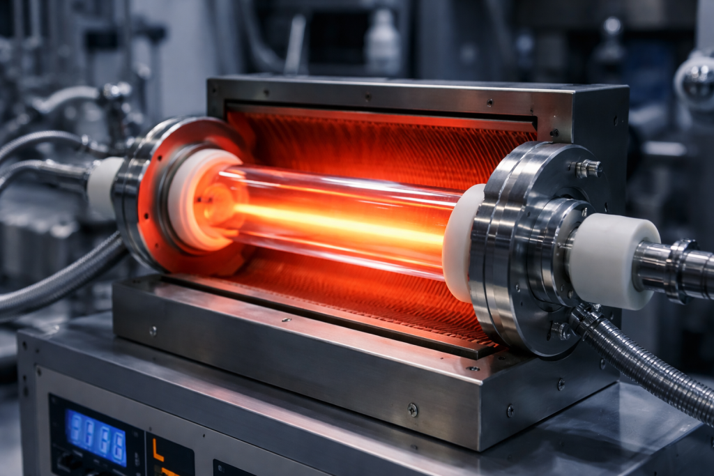
Glass substrates have long been indispensable materials in modern electronics, serving as the foundation for flat-panel displays, optical systems, and photomasks. However, the rapid growth of artificial intelligence (AI), high-performance computing (HPC), and advanced semiconductor packaging is transforming glass from a traditional display material into a strategic technology platform.
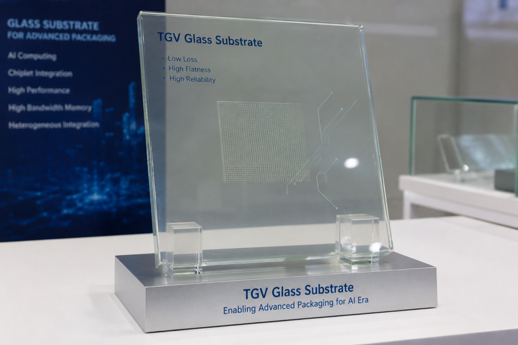
In particular, Through-Glass Via (TGV) glass substrates have emerged as one of the most promising next-generation packaging materials. Their unique electrical, thermal, and mechanical properties make them highly suitable for large AI processors, high-bandwidth memory (HBM), chiplet architectures, and co-packaged optics (CPO).
This article provides a comprehensive overview of the glass substrate industry, including its materials, manufacturing technologies, industrial value chain, market dynamics, and future prospects.
1. What Are Glass Substrates?
A glass substrate is a specially engineered glass material used as a supporting platform for electronic, optical, or semiconductor devices. Depending on the application, glass substrates can be categorized into four major segments:
- Display glass substrates
- Semiconductor TGV glass packaging substrates
- Quartz photomask substrates
- Automotive and optical specialty glass substrates
Among these categories, semiconductor glass substrates are attracting the greatest attention due to their potential role in next-generation AI computing systems.
2. The Glass Substrate Industry Value Chain
Upstream: Raw Materials and Manufacturing Equipment
High-Purity Quartz Materials
Quartz is the primary constituent of most advanced glass substrates and often accounts for the majority of material costs.
High-end semiconductor and display applications require ultra-high-purity quartz with impurity levels measured in parts per billion. The purity of quartz directly affects:
- Dielectric loss
- Thermal stability
- Optical transmission
- Electrical reliability
As device frequencies continue to increase, the demand for ultra-pure raw materials becomes increasingly critical.
Functional Additives
Specialized additives are introduced to tailor glass properties, including:
- Коэффициент теплового расширения
- Softening temperature
- Mechanical strength
- Optical characteristics
These additives enable the production of low-expansion, low-loss, and high-stability glass formulations required for advanced electronics.
Production Equipment
Glass substrate manufacturing relies on highly sophisticated equipment such as:
- Overflow fusion forming systems
- High-temperature melting furnaces
- Precision polishing equipment
- Ultrafast laser drilling systems
- Vacuum metallization tools
- Advanced inspection systems
The complexity of these manufacturing tools creates substantial barriers to entry for new participants.
Midstream: Glass Substrate Manufacturing
The midstream segment consists of two major processes:
Glass Sheet Production
This stage produces ultra-flat glass panels with precise thickness control.
Critical requirements include:
- Чрезвычайно низкая шероховатость поверхности
- High dimensional stability
- Minimal thermal expansion variation
- Exceptional purity
Advanced display panels and semiconductor packaging substrates both depend on these characteristics.
TGV Deep Processing
For semiconductor applications, glass substrates undergo additional processing steps:
- Glass thinning
- Laser drilling of microvias
- Via metallization
- Redistribution layer (RDL) fabrication
- Шлифование и полировка
- Final dicing
This stage represents one of the highest value-added portions of the entire supply chain.
Downstream Applications
1. Advanced Semiconductor Packaging
This is expected to become the fastest-growing application segment.
Key applications include:
- AI accelerators
- High-performance GPUs
- High-bandwidth memory
- Chiplet architectures
- 2.5D and 3D packaging
- Co-packaged optics
As semiconductor scaling becomes increasingly difficult and expensive, advanced packaging has become a major driver of performance improvement.
Glass substrates are viewed as a critical enabling technology for this transition.
2. Display Industry
Display glass remains the largest market segment by volume.
Приложения включают:
- LCD televisions
- OLED smartphones
- Monitors
- Tablets
- Foldable displays
While growth is relatively moderate, display substrates continue to provide a stable foundation for the industry.
3. Automotive Electronics
Modern vehicles increasingly rely on large digital displays and advanced sensing systems.
Приложения включают:
- Digital dashboards
- Head-up displays (HUD)
- Camera modules
- LiDAR systems
- Autonomous driving processors
Automotive qualification standards create high barriers to entry and long product lifecycles.
4. Photomask Substrates
Photomasks are essential tools in semiconductor lithography.
Ultra-high-purity quartz substrates are required for advanced photomask production due to their:
- Optical transparency
- Thermal stability
- Точность размеров
These products represent one of the highest technical barriers within the glass materials industry.
3. Why TGV Glass Substrates Matter for AI Computing
The Packaging Challenge
Modern AI processors continue to grow in size and complexity.
Current systems increasingly require:
- Multiple chiplets
- Massive memory bandwidth
- Larger package dimensions
- Higher signal frequencies
- Improved thermal management
Traditional packaging materials face growing limitations under these requirements.
Преимущества стеклянных подложек
Thermal Expansion Compatibility
Glass exhibits a thermal expansion coefficient close to that of silicon.
This reduces:
- Package warpage
- Mechanical stress
- Reliability issues
particularly in large-area packages.
Superior Electrical Performance
Glass offers:
- Low dielectric loss
- Excellent signal integrity
- Reduced power consumption
These characteristics become increasingly important at frequencies exceeding 100 GHz.
Larger Panel Sizes
Unlike silicon interposers, glass can be manufactured in larger panel formats.
This enables:
- Better material utilization
- Более низкая стоимость производства
- Higher throughput
for future panel-level packaging technologies.
Improved Mechanical Stability
Glass provides a rigid and dimensionally stable platform suitable for:
- Multi-chip integration
- Интерконнекты высокой плотности
- Advanced memory stacking
4. Current Industry Challenges
Despite its advantages, glass substrate technology still faces several technical hurdles.
Glass Manufacturing Complexity
Producing semiconductor-grade glass requires:
- Extremely precise compositions
- Tight thickness tolerances
- Ultra-low defect densities
Yield improvement remains a major challenge.
TGV Processing Difficulty
Creating thousands of microscopic vias in ultra-thin glass is technically demanding.
Основные задачи включают:
- Crack prevention
- Via quality control
- Metallization reliability
- Yield management
Even minor defects can significantly affect device performance.
Long Qualification Cycles
Semiconductor manufacturers typically require extensive reliability testing before adopting new packaging materials.
Qualification periods can extend from one to several years.
High Capital Investment
A complete glass substrate production line requires substantial investment in equipment and infrastructure.
This limits the number of companies capable of participating in the industry.
5. Market Outlook Through 2030
Industry analysts generally expect three phases of development.
Phase 1: Validation and Pilot Production (2026–2027)
Key characteristics:
- Technology qualification
- Pilot production lines
- Initial deployment in optical communication systems
- Small-volume AI packaging adoption
The focus remains on proving manufacturability and reliability.
Phase 2: Rapid Commercial Expansion (2028–2029)
Expected developments include:
- Large-scale adoption in AI processors
- Increased use in HBM packaging
- Expansion of panel-level packaging
- Accelerated supply-chain localization
This period could represent the fastest growth phase for semiconductor glass substrates.
Phase 3: Industry Maturity (2030 and Beyond)
Long-term trends may include:
- Sub-100 μm ultra-thin glass substrates
- Sub-micron via technologies
- Hybrid glass-organic package architectures
- Broader adoption in automotive, AR/VR, and edge computing devices
Glass substrates are expected to become a standard component in high-performance packaging platforms.
6. Future Technology Trends
Several important technological directions are emerging.
Ultra-Thin Glass
Future substrates are expected to become thinner while maintaining mechanical reliability.
Higher Via Density
Advances in laser processing will enable:
- Smaller via diameters
- Higher interconnect density
- Improved package performance
Hybrid Package Structures
Future systems may combine:
- Glass cores
- Organic redistribution layers
- Advanced interconnect architectures
to balance cost, performance, and manufacturability.
AI-Driven Demand Growth
The continuing expansion of AI infrastructure will remain the most important long-term demand driver for advanced glass packaging solutions.
Заключение
Glass substrates are transitioning from a mature display material into a strategic platform for next-generation semiconductor packaging. While display applications continue to provide a stable market foundation, the emergence of TGV glass substrates is creating entirely new growth opportunities driven by AI computing, high-bandwidth memory, chiplet integration, and co-packaged optics.
Although significant challenges remain in materials engineering, manufacturing yield, and industrial scaling, glass-based packaging technologies offer compelling advantages in signal integrity, thermal stability, scalability, and cost efficiency. As advanced packaging becomes increasingly important in the post-Moore era, glass substrates are positioned to become one of the most influential materials shaping the future of the global semiconductor industry.