Quartz wafer buyers often focus on diameter, thickness, surface roughness, total thickness variation, bow and warp. However, the condition of the wafer edge can be equally important, especially when the wafer will undergo coating, bonding, lithography, etching, cleaning, dicing or automated handling.
A quartz wafer may have an excellent polished surface but still fail during processing because of an unsuitable edge profile, excessive chipping, hidden cracks or an unclear edge exclusion requirement. These problems can increase particle generation, reduce usable area and create a risk of wafer breakage during transportation or processing.
This guide explains how to specify quartz wafer bevel geometry, edge exclusion, chipping limits and inspection requirements when preparing a purchase specification or RFQ.
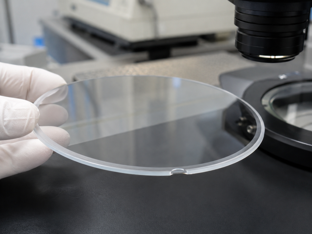
Why Quartz Wafer Edge Quality Matters
The edge is one of the most mechanically vulnerable areas of a quartz wafer. Cutting, grinding, lapping and polishing can leave small chips, sharp transitions or subsurface damage around the perimeter.
During subsequent processing, the wafer edge may contact:
- Wafer cassettes
- Vacuum chucks
- Edge-grip end effectors
- Bonding fixtures
- Cleaning equipment
- Spin-coating tools
- Dicing tape and mounting frames
- Manual handling tools
A properly shaped edge helps reduce local stress concentration and lowers the probability of chipping during handling. In semiconductor wafer standards, deliberate edge contouring is used to reduce chipping and limit problems such as edge crown and photoresist edge bead. Although these standards were originally developed for semiconductor wafers, the same basic edge-control principles can also be useful for quartz and fused silica substrates.
Edge quality can affect four major areas:
- Mechanical strength: Large chips and microcracks can become fracture origins.
- Particle control: Loose fragments or damaged edge regions may generate particles.
- Process compatibility: Poor edge geometry can interfere with coating, bonding and automated handling.
- Usable surface area: Edge exclusion determines how close functional patterns or measurements can extend toward the perimeter.
For these reasons, edge quality should be specified separately from front-surface scratch-dig, roughness or flatness requirements.
1. Quartz Wafer Bevel and Edge Profile
The term “bevel” is sometimes used broadly to describe any intentionally shaped wafer edge. However, several different profiles may be supplied.
Chamfered Edge
A chamfer removes the sharp corner between the polished surface and the wafer perimeter. It usually creates one or more flat angled surfaces.
Chamfered edges are often used when:
- The wafer is relatively thick
- A simple protective edge is sufficient
- The final process does not require a semiconductor-style rounded profile
- Cost control is important
- The substrate will be manually loaded or mounted
A drawing should specify the chamfer width, angle and whether both the front and back edges must be processed.
Rounded Edge
A rounded edge creates a curved transition between the front surface, outer diameter and back surface. It may provide a smoother stress transition than a sharp or minimally chamfered edge.
Rounded edges are generally considered for:
- Automated wafer handling
- Repeated cleaning cycles
- Wafer bonding
- Spin coating
- Thin quartz wafers
- Applications with strict breakage control
Double-Side Bevel
A double-side bevel removes material from both the front and rear perimeter. The two bevels meet near the maximum wafer diameter.
The customer should specify whether the profile must be:
- Symmetrical
- Front-side dominant
- Back-side dominant
- Rounded at the apex
- Flat at the apex
- Controlled by a reference profile or drawing
Edge Profile Parameters
A detailed edge profile can include:
- Front bevel angle
- Back bevel angle
- Front bevel width
- Back bevel width
- Apex width
- Apex radius
- Shoulder radius
- Edge roundness
- Maximum diameter location
- Transition position between the polished face and bevel
SEMI M73 identifies characteristics such as bevel angles, edge widths, apex dimensions, shoulder radii and edge roundness for measured wafer edge profiles. The standard is written for silicon wafers but states that its methods may also be applied to wafers made from other materials. For quartz wafers, the supplier and buyer should agree on the profile, measurement position and acceptance limits.
2. What Is Edge Exclusion?
Edge exclusion is a band around the outer perimeter of the wafer in which specified surface or geometry requirements do not apply.
SEMI terminology defines edge exclusion as the width of a narrow band located inside the wafer edge. The central area inside this band is commonly referred to as the fixed quality area, or FQA.
For example, when a customer specifies:
- Wafer diameter: 150 mm
- Edge exclusion: 3 mm
the controlled quality area generally extends to a diameter of approximately:
150 mm − 2 × 3 mm = 144 mm
However, the exact interpretation must be stated in the drawing or specification. Customers should clarify whether edge exclusion applies to:
- Surface roughness
- Scratch-dig quality
- Flatness
- TTV measurement
- Coating coverage
- Patterning
- Particle inspection
- Cosmetic defects
- Chipping acceptance
- Bonding area
Edge exclusion does not automatically mean that severe chips or cracks are acceptable inside the excluded band. Structural defects should have separate acceptance criteria.
Edge Exclusion Is Not the Same as Bevel Width
These two terms are related but not interchangeable.
Bevel width describes the physical shaped area of the wafer edge.
Edge exclusion describes the surface region excluded from specified quality or process requirements.
For example, a wafer may have a 0.5 mm physical bevel but a 3 mm edge exclusion for flatness, coating or device patterning.
How to Select an Edge Exclusion Value
The correct edge exclusion depends on the downstream process.
A smaller exclusion provides more usable wafer area but may require:
- Better near-edge flatness
- Tighter bevel control
- Lower chipping
- More precise coating
- Improved edge inspection
- Better control of edge roll-off
- More advanced handling equipment
A larger exclusion may simplify processing but reduces the usable area.
The buyer should confirm the minimum process margin with the lithography, coating, bonding or inspection equipment supplier before fixing the requirement.
3. Quartz Wafer Chipping Requirements
Chipping refers to localized material loss at or near the wafer perimeter. Chipping may be created during cutting, edge grinding, polishing, cleaning, packaging or transport.
Not all chips have the same risk. A useful chipping specification should consider several dimensions.
Radial Intrusion
Radial intrusion is the distance that a chip extends inward from the nominal wafer perimeter.
This dimension is important because it determines whether the chip enters the usable surface area or fixed quality area.
Tangential Length
Tangential length describes how far the defect extends along the wafer circumference.
A chip with limited radial depth but a long circumferential length may still indicate unstable edge processing.
Vertical Depth
Vertical depth describes how far the chip penetrates through the wafer thickness or into the bevel.
For thin quartz wafers, a deep chip can significantly reduce the remaining load-bearing cross-section.
Chip Count
A specification may define:
- Maximum number of chips per wafer
- Maximum number above a specified size
- Total cumulative chip length
- Different limits for major and minor chips
- Zero allowance for chips entering the FQA
Edge Cracks
A crack is different from a simple open chip. It may extend below the visible surface and can propagate during thermal cycling, mechanical loading or cleaning.
For critical applications, the usual purchasing requirement should be:
No visible edge cracks permitted.
A chip may be accepted within an agreed size limit, but a crack extending from the chip should normally be treated separately.
SEMI wafer specification documents distinguish between edge chips, edge indents, edge cracks and other surface defects, demonstrating why a purchase specification should not group all edge damage under one general term.
4. Typical Causes of Quartz Wafer Edge Chipping
Edge defects can originate from several manufacturing and handling stages.
Cutting Damage
Mechanical sawing may create rough edge regions, microcracks or localized breakouts if the blade, feed rate, coolant or support condition is unsuitable.
Laser-based cutting processes can reduce kerf loss and particle generation when properly optimized. Corning reports that laser processing of fused silica wafers can achieve precise edges and controlled chipping, illustrating how strongly the cutting method affects final edge quality.
Edge Grinding
An aggressive grinding rate, worn wheel, unsuitable abrasive size or inadequate cooling can leave large chips or subsurface damage.
Lapping and Polishing
Improper support during thinning may create edge stress. Thin wafers are especially sensitive because their edges can flex during polishing and cleaning.
Cleaning
High-pressure spray, ultrasonic energy, cassette contact or rapid temperature changes may enlarge existing defects.
Packaging and Shipping
Direct wafer-to-wafer contact, unsuitable separators or excessive movement inside the shipping cassette can create new chips after final inspection.
The inspection report should therefore represent the condition after final cleaning and before shipment, not only the condition immediately after edge grinding.
5. Quartz Wafer Edge Inspection Methods
A complete inspection plan may combine visual examination, microscopy and profile measurement.
Visual Inspection
Visual inspection under controlled lighting can identify:
- Large edge chips
- Cracks
- Saw marks
- Stains
- Residue
- Irregular beveling
- Major diameter damage
Visual inspection is useful for routine production but may not detect small or low-contrast defects.
The inspection conditions should define:
- Light source
- Background
- Magnification
- Viewing angle
- Operator qualification
- Minimum detectable defect
- Sampling or 100% inspection
Optical Microscope Inspection
Microscope inspection is appropriate when the customer specifies a maximum chip size in micrometers.
The inspection should record:
- Maximum radial intrusion
- Tangential length
- Defect location
- Number of defects
- Presence or absence of cracks
- Representative photographs
A calibrated measurement scale should be used rather than estimating defect size visually.
360-Degree Edge Imaging
Automated or semi-automated systems can rotate the wafer and inspect the full perimeter. Such systems can examine the front bevel, apex, back bevel and near-edge surface.
Commercial semiconductor inspection platforms may combine edge defect inspection, edge profile measurement and film-edge metrology in one system.
This approach is suitable for:
- High-volume production
- Tight chipping limits
- Automated defect classification
- Traceable wafer-by-wafer reports
- High-value bonding or photonics applications
Edge Profile Measurement
A profile measurement checks whether the produced bevel conforms to the specified geometry.
Possible methods include:
- Optical profile measurement
- White-light interferometry
- Confocal measurement
- Stylus profilometry
- Shadow imaging
- Template comparison
- Cross-sectional measurement on qualification samples
The selected method must be compatible with transparent quartz. Reflections from the front, rear and bevel surfaces can complicate optical measurement, so fixture design and measurement settings should be validated.
Non-contact optical and AFM-based metrology systems are available for bevel-edge profiling, near-edge topography and structural measurements.
Polarized-Light Inspection
Polarized-light inspection may be useful for evaluating residual stress patterns in transparent quartz parts. It does not replace direct chip or crack measurement, but it can provide supplementary information when edge machining or thermal processing may have introduced stress.
6. How to Specify Edge Quality in an RFQ
Avoid writing only:
“Good edge quality required.”
This statement is subjective and cannot be inspected consistently.
A more complete RFQ should include the following items.
| Specification item | Information to provide |
|---|---|
| Material | Fused quartz, synthetic fused silica or specified grade |
| Wafer diameter | Nominal diameter and tolerance |
| Wafer thickness | Nominal thickness and tolerance |
| Edge profile | Chamfered, rounded, double bevel or drawing-controlled |
| Front bevel | Width, angle or radius |
| Back bevel | Width, angle or radius |
| Apex | Width, radius or acceptable profile |
| Edge exclusion | Width and affected parameters |
| Maximum chip size | Radial, tangential and depth limits |
| Chip quantity | Maximum count per wafer |
| Edge cracks | None permitted or defined acceptance |
| FQA requirement | No chips entering the FQA |
| Inspection | Visual, microscope, profile measurement or automated scan |
| Sampling | 100% or agreed sampling plan |
| Report | Summary report, wafer map or defect photographs |
| Packaging | Individual separator, cassette type and clean packaging |
Example Quartz Wafer Edge Specification
A practical drawing note may be written as follows:
Edge profile: Double-side rounded bevel according to approved drawing.
Edge exclusion: 3.0 mm from the nominal wafer perimeter. Edge exclusion applies to surface quality, flatness and coating coverage unless otherwise specified.
Chipping: Maximum permitted chip dimensions shall be defined by radial intrusion, tangential length and vertical depth.
Fixed quality area: No chip, crack or fracture may enter the specified quality area.
Cracks: No visible edge cracks permitted under the agreed inspection magnification.
Inspection: 100% visual edge inspection after final cleaning. Microscope measurement is required for defects approaching the acceptance limit.
Documentation: Inspection report to include maximum recorded chip size and representative photographs when requested.
The actual numeric limits should be selected according to wafer diameter, thickness and application rather than copied from an unrelated silicon wafer specification.
7. Edge Requirements for Different Applications
Quartz Carrier Wafers
Carrier wafers used for temporary bonding require stable handling and controlled near-edge geometry. The buyer should define whether adhesive, wax or bonding film may extend into the edge exclusion zone.
Optical Quartz Wafers
Optical applications may require a polished or visually uniform bevel, particularly when stray light, scattering or cosmetic appearance is important.
MEMS and Wafer-Level Packaging
Bonding applications often need tight control of the usable bonding area, edge exclusion, particle condition and bevel transition. Edge chips that do not break the wafer may still interfere with sealing or bonding fixtures.
Coated Quartz Wafers
The specification should clarify whether the coating must:
- Stop before the bevel
- Cover part of the bevel
- Extend to the nominal edge
- Maintain a defined edge clearance
- Avoid edge bead or coating buildup
Thin Quartz Wafers
As wafer thickness decreases, edge damage becomes more critical. Thin wafers may require:
- Larger protective bevels
- Reduced handling force
- Individual packaging
- Temporary carrier bonding
- Tighter chip limits
- Full-perimeter inspection
8. Common Purchasing Mistakes
Specifying Only “SEMI Standard Edge”
This wording may be unclear because SEMI edge standards are primarily written around specific semiconductor wafer materials and dimensions.
For quartz wafers, attach a profile drawing or approved sample.
Using Only One Chip Dimension
A chip should not be described only by length. Radial intrusion and vertical depth may be more important than the visible circumferential length.
Treating Edge Exclusion as a Defect Zone
Edge exclusion does not automatically permit unlimited chipping, cracks or contamination.
Ignoring the Back Bevel
Some drawings specify only the front-side bevel. Back-edge geometry can still affect vacuum chucking, cassette contact and wafer bonding.
Omitting the Inspection Method
A 20 µm defect limit is not meaningful unless the inspection equipment can reliably detect and measure defects at that level.
Requiring Zero Chipping Without Defining Detection Limits
“Zero chipping” may be interpreted differently under unaided visual inspection, 10× microscopy and automated optical inspection.
A better requirement is:
“No edge chips larger than the specified dimensions when inspected using the agreed method and magnification.”
Conclusion
Quartz wafer edge quality should be treated as a measurable engineering requirement rather than a cosmetic preference.
A complete specification should define:
- Bevel or edge profile
- Edge exclusion
- Fixed quality area
- Maximum chip dimensions
- Chip quantity
- Crack acceptance
- Inspection method
- Sampling plan
- Inspection report
- Packaging method
The most effective approach is to provide the quartz wafer supplier with a drawing, downstream process conditions and clearly defined acceptance criteria. This allows the edge grinding, polishing, cleaning and inspection processes to be matched to the actual application.
Frequently Asked Questions
Is a beveled edge required for every quartz wafer?
Not necessarily. Thick substrates used in simple laboratory applications may only require a basic chamfer. Thin wafers, bonded wafers and substrates used in automated semiconductor equipment usually benefit from a more carefully controlled edge profile.
What is the difference between edge exclusion and edge chipping?
Edge exclusion is a defined perimeter band where certain surface or geometry specifications may not apply. Edge chipping is physical material loss. A chip may still be rejected even when it is located inside the edge exclusion zone.
Should quartz wafer edges be polished?
Edge polishing may improve cleanliness, appearance and edge condition, but it increases processing cost. The required finish depends on whether the wafer will be bonded, coated, repeatedly cleaned or handled automatically.
Can silicon wafer edge standards be used for quartz wafers?
They can be used as technical references, but they should not be applied automatically. Quartz material behavior, thickness, transparency and processing conditions differ from silicon. The supplier and buyer should agree on the profile and inspection criteria.
What information should be included in an edge inspection report?
The report may include wafer identification, inspection method, magnification, maximum chip size, chip count, crack result, bevel profile measurements and defect photographs.