
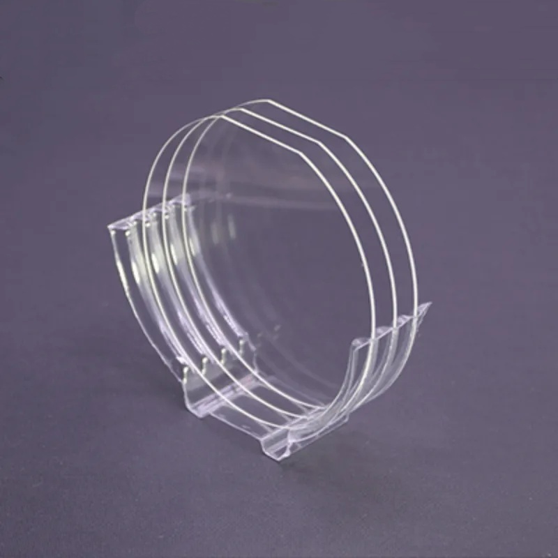
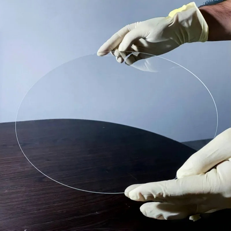
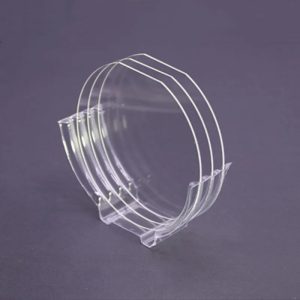
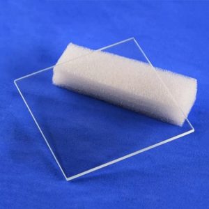
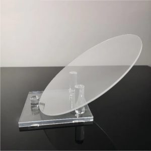
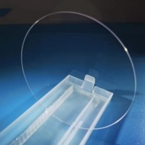
 FUYAO QUARTZ specializes in high-purity BF33 / BOROFLOAT 33 glass wafers, a premium borosilicate substrate widely used in semiconductor, MEMS, optical, and microfluidic applications. Manufactured via SCHOTT’s microfloat process, BF33 wafers feature low thermal expansion (~3.3 ppm/°C), high optical clarity, thermal shock resistance, and chemical inertness, making them ideal for precision bonding with silicon and other advanced processes.
BF33 wafers are widely adopted in photolithography, anodic bonding, lab-on-chip devices, laser optics, and high-temperature optical systems, providing exceptional performance and reliability under demanding industrial and scientific conditions.
Material Composition & Properties
| Property | Specification |
|---|---|
| SiO₂ Content | >80% |
| B₂O₃ Content | Optimized for low thermal expansion |
| CTE (20–300°C) | ~3.3 × 10⁻⁶ /K |
| Strain Point | 520°C |
| Annealing Point | 560°C |
| Softening Point | 820°C |
| Thermal Shock Resistance | Excellent |
| Optical Transmission | >90% (UV–NIR) |
| Surface Finish | DSP/SSP, Ra <1 nm |
| Chemical Resistance | ISO Class 1 water & acid, Class 2 alkali |
| Hardness | ~480 HK |
Key Advantages:
-
Thermal Compatibility with Silicon: Ideal for anodic bonding without stress or deformation.
-
High Optical Clarity: UV–NIR transparency for lasers, photonics, and sensors.
-
Chemical Durability: Resistant to acids, bases, and solvents for cleanroom processes.
-
Mechanical Strength: High abrasion resistance, ideal for semiconductor handling and MEMS devices.
-
Precision Surface: Polished wafers with low TTV for accurate microfabrication and optical alignment.
Primary Applications
-
Semiconductor & MEMS: Carrier wafers, wafer thinning, anodic bonding, microfluidic devices.
-
Optical & Photonic Systems: Laser optics, mirrors, filters, high-temperature optical windows.
-
Analytical & Biomedical Instruments: Biochips, diagnostic plates, titration systems.
-
Industrial & High-Temperature Environments: Kiln windows, sight glasses, floodlight covers.
-
Energy & Environmental Technology: PV substrates, microfluidic sensors.
-
Aerospace & Defense: Optical panels, sensor windows, space-grade optics.
Surface & Fabrication Options
-
Polishing: Double-side polished (DSP) or single-side polished (SSP) with Ra <1 nm.
-
Thickness & Diameter: Customizable per application.
-
Coatings: Anti-reflection (AR), reflective (HR), wavelength-specific coatings.
-
Tolerance: Tight TTV (<10 µm), scratch/dig 60/40 or higher upon request.
Why Choose Our BF33 Wafers?
-
Decades of experience in optical and semiconductor glass manufacturing.
-
Strict quality control for consistency in thermal, chemical, and optical properties.
-
Flexible customization to meet industrial, scientific, and R&D requirements.
-
Comprehensive technical support and global delivery network.
Frequently Asked Questions (FAQ)
Q1: What is BF33 glass?
A1: BF33, also called BOROFLOAT 33, is a high-quality borosilicate glass wafer with low thermal expansion (~3.3 ppm/°C), excellent chemical durability, and high optical transparency, ideal for semiconductor, MEMS, and optical applications.
Q2: How does BF33 compare to ordinary glass?
A2: BF33 has higher silica content (>80%) and boron oxide, giving it low thermal expansion, chemical resistance, superior UV/NIR transmission, and mechanical strength, outperforming soda-lime glass in demanding industrial applications.
Q3: Can BF33 wafers be polished?
A3: Yes. FUYAO QUARTZ provides DSP and SSP wafers with sub-nanometer surface roughness (<1 nm Ra) and low TTV (<10 µm), essential for wafer bonding, photolithography, and high-precision optical systems.
Q4: What industries use BF33 wafers?
A4: Semiconductor fabrication, MEMS devices, microfluidics, photonics, laser optics, analytical instruments, biomedical devices, aerospace, energy, and environmental monitoring.


Reviews
There are no reviews yet.