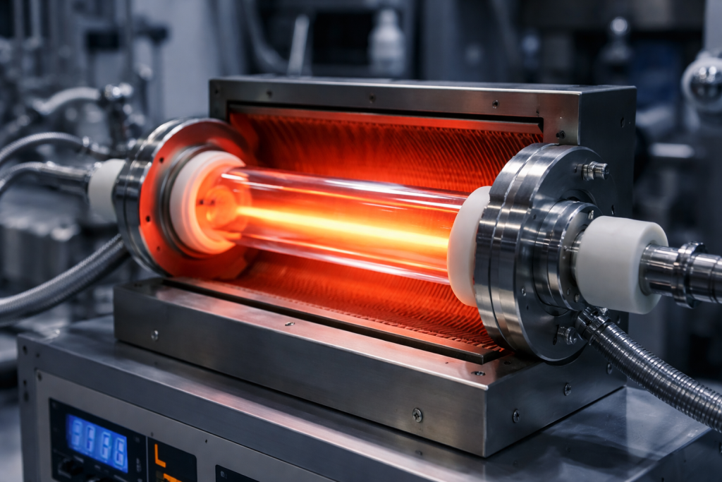
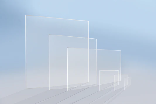
BF33 glass wafer is a high-performance borosilicate glass substrate widely used in semiconductor processing, MEMS devices, optical components, microfluidic chips, wafer bonding, and laboratory-grade precision applications. Compared with ordinary soda-lime glass, BF33 offers better thermal stability, lower thermal expansion, higher chemical resistance, and more reliable dimensional control during heating and cooling cycles.
For engineers, buyers, and R&D teams, selecting the right glass wafer is not only about size or thickness. Key material properties such as coefficient of thermal expansion, optical transmission, surface quality, thermal resistance, and chemical durability all directly affect processing yield and device performance. This article explains the core properties of BF33 glass wafers and why this material is often chosen for advanced technical applications.

What Is BF33 Glass Wafer?
BF33 is a borosilicate glass material with a composition rich in silicon dioxide and boron oxide. It is known for its low thermal expansion, high optical clarity, stable chemical performance, and good process compatibility. In wafer form, BF33 glass is manufactured into round or square substrates with controlled thickness, surface roughness, flatness, edge quality, and dimensional tolerance.
Typical BF33 glass wafers are available in different diameters, such as 2 inch, 3 inch, 4 inch, 6 inch, 8 inch, and customized sizes. Depending on the application, the wafer can be supplied as single-side polished, double-side polished, ground, diced, drilled, or custom-shaped.
In many technical applications, BF33 is selected as a cost-effective alternative to fused silica or quartz when ultra-deep UV transmission is not required but high thermal stability and precision processing are still important.
Coefficient of Thermal Expansion: Why CTE Matters
One of the most important properties of BF33 glass wafer is its low coefficient of thermal expansion, commonly around 3.3 × 10⁻⁶/K within a typical temperature range. This means the material expands only slightly when heated and contracts predictably when cooled.
Low CTE is especially important in processes involving temperature changes, such as anodic bonding, wafer-level packaging, thin-film deposition, lithography, thermal cycling, and MEMS fabrication. If the glass substrate expands too much, it may cause stress, warpage, cracking, film delamination, or bonding failure.
BF33’s low CTE makes it suitable for applications where dimensional stability is required. For example, in MEMS devices, a glass wafer may be bonded to silicon. Since the thermal expansion of BF33 is relatively close to that of silicon, thermal stress can be better controlled during bonding and later device operation.
This is one reason BF33 glass wafers are often used in pressure sensors, microfluidic devices, optical windows, wafer bonding substrates, and precision carrier wafers.
Optical Transmission Performance
BF33 glass wafer also offers excellent optical transparency in the visible light range. Depending on thickness, surface finish, and wavelength, BF33 can typically achieve high visible light transmission, often above 90% for polished thin wafers.
This makes it useful for optical observation windows, sensor covers, transparent substrates, display-related components, laboratory inspection plates, and microfluidic chips where visual monitoring is required.
However, it is important to understand that BF33 is not the same as fused silica or synthetic quartz in optical performance. Fused silica generally provides better ultraviolet transmission, especially in deep-UV applications. BF33 is more suitable for visible and near-infrared applications where cost, thermal stability, processability, and chemical resistance are more important than extreme UV transparency.
For applications requiring 193 nm, 248 nm, or other deep-UV optical performance, fused silica may be a better option. But for general optical windows, MEMS covers, microfluidic observation substrates, and visible light inspection, BF33 glass wafer can be an efficient and economical choice.
Thermal Stability and Working Temperature
BF33 glass is well known for its thermal resistance. It has a relatively high softening point, typically around 820°C, with annealing and strain points often around 560°C and 520°C respectively. These values indicate that BF33 can maintain structural stability under many thermal processing conditions.
In practical use, the long-term working temperature should always be lower than the softening point. The actual usable temperature depends on wafer thickness, heating rate, cooling rate, fixture design, atmosphere, mechanical load, and whether the wafer is bonded or coated.
The key advantage of BF33 is not only that it can withstand heat, but that it can handle temperature changes with relatively low stress. This makes it suitable for repeated heating and cooling cycles where ordinary glass may crack or deform.
In wafer-level processing, thermal stability affects the reliability of the entire structure. A glass wafer with poor thermal resistance may bend, warp, or develop internal stress during processing. BF33 helps reduce these risks and provides a stable platform for high-precision applications.
Chemische weerstand
BF33 borosilicate glass offers better chemical resistance than standard soda-lime glass. It performs well in many acidic and neutral environments and is commonly used in laboratory glassware, analytical instruments, and technical substrates.
For wafer applications, chemical resistance is important during cleaning, wet processing, bonding preparation, and microfabrication. Surface contamination, corrosion, or chemical attack can affect bonding quality, film adhesion, optical clarity, and device reliability.
Although BF33 has good chemical durability, it is still necessary to evaluate the actual process chemistry. Strong alkaline solutions, hydrofluoric acid, and certain aggressive etchants may attack the glass surface. For semiconductor or MEMS applications, process compatibility should be confirmed before mass production.
Surface Quality and Wafer Processing
BF33 glass wafer can be processed with high surface quality. Depending on the application, wafers may be supplied with polished surfaces, controlled roughness, low total thickness variation, and precision edge finishing.
For optical and bonding applications, double-side polished BF33 wafers are often preferred. A smooth surface helps improve optical clarity, bonding uniformity, and thin-film deposition quality. For some applications, surface roughness can reach the nanometer level, depending on polishing capability and specification requirements.
Important wafer parameters include diameter, thickness, thickness tolerance, TTV, bow, warp, surface roughness, edge chamfer, and particle control. These parameters should be clearly defined when ordering BF33 glass wafers, especially for semiconductor, MEMS, and optical packaging applications.
A small difference in flatness or thickness variation may not matter for general laboratory use, but it can become critical in wafer bonding, lithography, and thin-film coating processes.
BF33 Glass Wafer vs Soda-Lime Glass Wafer
Compared with soda-lime glass, BF33 has lower thermal expansion, better thermal shock resistance, stronger chemical durability, and more stable optical performance. Soda-lime glass is often cheaper and suitable for simple display, cover, or non-critical applications. However, it may not perform well in processes involving high temperature, chemical exposure, or precision bonding.
BF33 is usually preferred when the wafer must maintain dimensional stability and survive thermal cycling. For R&D labs and production environments, the higher material cost of BF33 can often be justified by improved reliability and lower process failure risk.
BF33 Glass Wafer vs Fused Silica Wafer
Fused silica offers superior UV transmission, higher purity, lower thermal expansion, and better high-temperature performance. It is widely used in demanding optical, semiconductor, and photonics applications. However, fused silica is generally more expensive and more difficult to process.
BF33 is a practical choice when the application does not require the extreme performance of fused silica. It provides a good balance between cost, thermal stability, optical transparency, and processing flexibility.
For example, if the application is visible light inspection, MEMS packaging, microfluidic chip fabrication, or general wafer bonding, BF33 may be sufficient. If the application involves deep UV optics, high-purity semiconductor processing, or extreme thermal environments, fused silica or quartz may be more suitable.
Typical Applications of BF33 Glass Wafers
BF33 glass wafers are used in many industries where transparency, stability, and precision are required. Common applications include MEMS sensor packaging, anodic bonding, microfluidic chips, biomedical analysis devices, optical windows, laboratory substrates, semiconductor carrier wafers, thin-film deposition substrates, display research, and precision inspection plates.
In MEMS packaging, BF33 can serve as a cover wafer or bonding substrate. In microfluidics, its transparency allows direct observation of fluid channels. In optical systems, polished BF33 wafers can function as protective windows or transparent support substrates. In R&D environments, BF33 wafers are often used for testing, prototyping, and process development.
How to Specify a BF33 Glass Wafer
When purchasing BF33 glass wafers, it is important to define the technical requirements clearly. The main specifications usually include wafer diameter or custom size, thickness, thickness tolerance, surface polishing condition, surface roughness, TTV, bow, warp, edge finish, hole or slot design, cleaning grade, and packaging requirements.
For bonding or lithography applications, double-side polishing, low roughness, and tight thickness control are usually required. For optical windows, transmission, surface quality, and edge processing should be emphasized. For microfluidic devices, additional processing such as drilling, dicing, channel fabrication, or bonding compatibility may be required.
Providing drawings, target application, operating temperature, chemical environment, and required tolerance can help manufacturers recommend the most suitable wafer specification.
Conclusie
BF33 glass wafer is a versatile borosilicate glass substrate with low thermal expansion, high visible light transmission, good thermal stability, and reliable chemical resistance. These properties make it suitable for MEMS, optical packaging, microfluidics, laboratory devices, wafer bonding, and precision technical applications.
Its coefficient of thermal expansion helps reduce thermal stress. Its optical transparency supports visible inspection and sensor applications. Its thermal stability allows it to withstand many heating and cooling processes. Compared with soda-lime glass, BF33 provides higher reliability. Compared with fused silica, it offers a more economical solution for applications that do not require extreme UV or ultra-high-temperature performance.
For engineers and buyers, choosing BF33 glass wafer means balancing performance, cost, and process requirements. By carefully specifying wafer size, thickness, polishing quality, flatness, and application environment, BF33 can provide a stable and efficient substrate solution for a wide range of advanced industrial and research applications.