
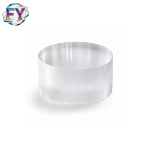
 The 6 inch JGS2 fused silica wafer is a high precision quartz substrate specifically engineered for advanced optical and semiconductor applications. Manufactured using UV grade JGS2 fused silica, this wafer offers excellent optical transmission, thermal stability, and mechanical strength, making it a reliable material for demanding industrial environments.
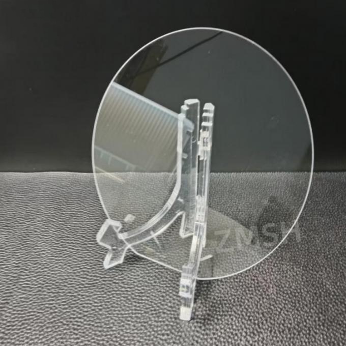
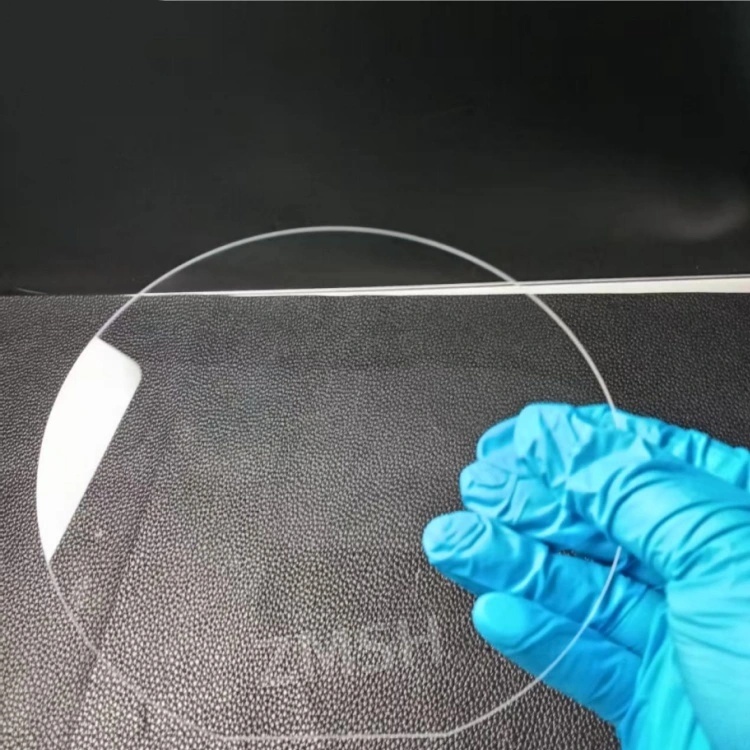
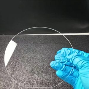
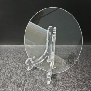
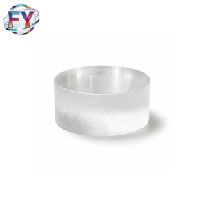
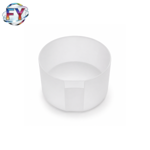
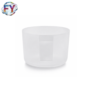
With a standard diameter of 150 mm and a thickness of 1 mm, the wafer is processed using double side polishing technology. This ensures both surfaces achieve high flatness and ultra low surface roughness, which is essential for minimizing optical distortion and improving system performance. The consistent quality and uniformity also support wafer level processing and high accuracy alignment requirements.
JGS2 fused silica is known for its wide transmission range from 220 nm to 2500 nm. This allows efficient transmission across ultraviolet, visible, and near infrared wavelengths, making it highly suitable for optical windows, photonic devices, and precision instruments. In addition, its extremely low thermal expansion coefficient ensures excellent dimensional stability under temperature variations and high energy exposure.
주요 기능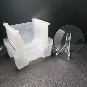
- Broad optical transmission range from 220 nm to 2500 nm
- Double side polished surface with high flatness and low roughness
- Ultra low thermal expansion for stable performance under heat
- High purity fused silica suitable for semiconductor processes
- Strong mechanical properties with reliable hardness and rigidity
- Excellent resistance to most chemical environments
기술 사양
| 매개변수 | 가치 |
|---|---|
| 지름 | 6 inch (150 mm) |
| 두께 | 1 mm |
| 재료 | JGS2 Fused Silica |
| 표면 마감 | Double Side Polished |
| 밀도 | ~2.2 g/cm³ |
| 경도 | Mohs ~7 |
| 영의 계수 | ~72 GPa |
| 열팽창 | ~5.5×10⁻⁷/°C |
| 전송 범위 | 220nm ~ 2500nm |
 재료 특성
재료 특성
JGS2 fused silica is produced through a hydrogen oxygen flame fusion process, resulting in a material with high purity and excellent structural uniformity. It is widely used in high end optical and semiconductor industries due to its stable and predictable performance.
One of the most important advantages of JGS2 is its superior optical transparency. It allows efficient transmission of light from deep ultraviolet to near infrared wavelengths, which is critical for optical systems requiring low loss and high precision.
Its extremely low coefficient of thermal expansion significantly reduces the risk of deformation or cracking during rapid temperature changes. This makes it highly suitable for applications involving high temperature processing or laser exposure.
In addition, JGS2 fused silica demonstrates strong chemical stability. It is resistant to most acids and industrial chemicals, ensuring long term durability in harsh environments. The combination of optical, thermal, and chemical stability makes it a preferred material for precision applications.
애플리케이션
The 6 inch JGS2 DSP quartz wafer is widely used across multiple high technology industries where precision and stability are essential.
In semiconductor manufacturing, it is commonly used as a carrier wafer or substrate in photolithography and etching processes. Its purity and thermal stability help maintain process consistency and yield.
In optical applications, it serves as a base material for high performance optical windows, filters, and lenses. Its ability to transmit UV light makes it especially valuable for ultraviolet optical systems.
In photonic communication, the wafer is used in the fabrication of DWDM filter substrates and other optical components that require low signal loss and high uniformity.
It is also suitable for laser systems, MEMS devices, and precision measurement equipment where dimensional stability and optical quality are critical.
자주 묻는 질문
Q1 What is the advantage of double side polishing for this wafer
Double side polishing improves both surface flatness and parallelism, which are critical for optical performance and wafer bonding processes. It reduces surface defects and scattering, ensuring higher transmission efficiency and better system accuracy.
Q2 Why is JGS2 fused silica suitable for UV applications
JGS2 offers strong transmission down to 220 nm, which is essential for ultraviolet optical systems. Its low impurity content minimizes absorption and ensures stable performance under prolonged UV exposure.
Q3 Is this wafer suitable for high temperature environments
Yes, due to its extremely low thermal expansion and high softening point, JGS2 fused silica can maintain dimensional stability and structural integrity even under high temperature conditions, making it suitable for semiconductor and laser applications.
상품평
아직 상품평이 없습니다.