
Aperçu du produit
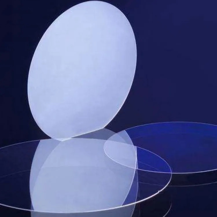
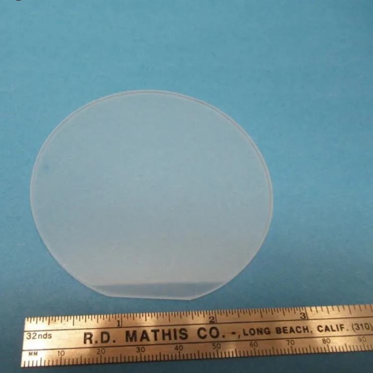
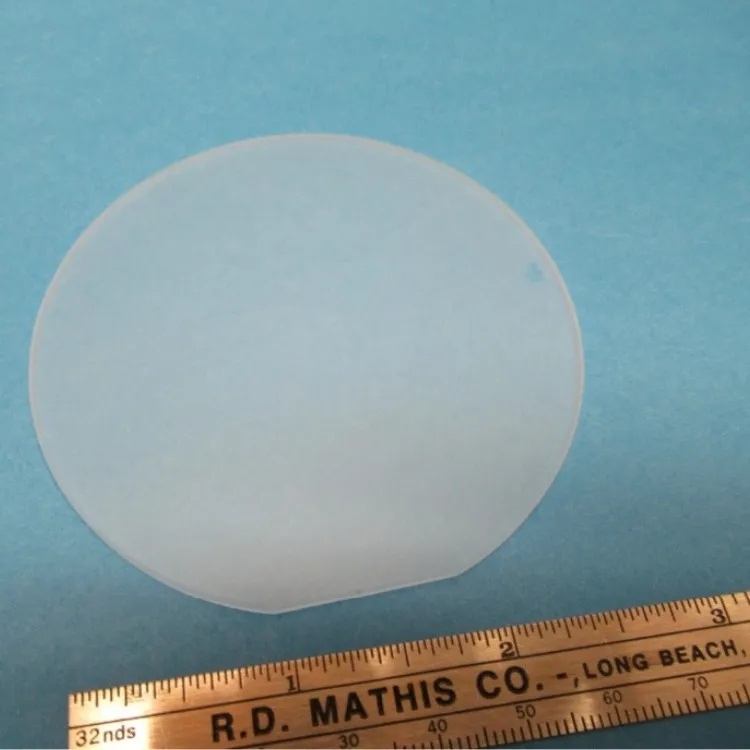
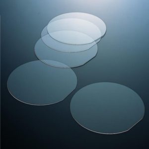
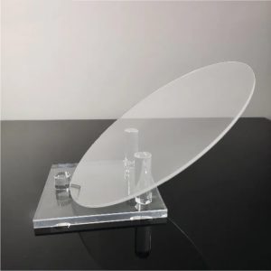
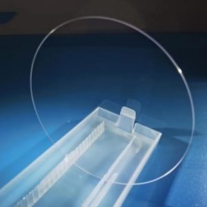
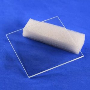
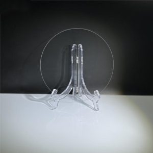 The 2-inch quartz wafer is a semiconductor-grade substrate made from high-purity silicon dioxide (SiO₂). It achieves micron-level flatness through precision processing techniques such as CNC cutting and laser polishing. These wafers comply with SEMI standards and support customization in dimensions and thickness (±0.02 mm tolerance), making them suitable for optoelectronics, MEMS (Micro-Electro-Mechanical Systems), and semiconductor packaging.
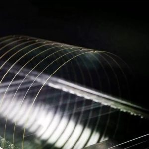
Fuyao provides customized production for non-standard geometries, including freeform shapes, graded thickness, and advanced surface treatments such as Anti-Reflective (AR) coatings and hydrophobic films. Full-process quality control ensures total thickness variation (TTV) <0.005 mm and surface roughness Ra <1.5 nm. Small-batch prototyping (minimum 10 units) and rapid delivery options are available for time-sensitive projects.
Spécifications
| Paramètres | Spécifications |
|---|---|
| Diamètre | 2 inch (50.8 mm) |
| Thickness Range | 0.1 mm – 1.0 mm |
| Material Purity | ≥99.99% |
| Surface Roughness (Ra) | ≤5 nm |
| Total Thickness Variation | ≤10 μm |
| Transmittance (@193 nm) | >90% |
| Coefficient of Thermal Expansion | ~0.55×10⁻⁶/°C |
| Point d'adoucissement | ~1665°C |
| Emballage | 100-Level Cleanroom |
1 Optical Excellence
-
Broad-Spectrum Transmittance: >90% in the ultraviolet range (185–3500 nm), with superior short-wave UV performance (185 nm).
-
Low Thermal Expansion: CTE ~0.52×10⁻⁶/°C (5–35°C), can withstand long-term temperatures up to 1100°C and short-term exposure to 1450°C.
2 Mechanical and Chemical Stability
-
High Strength: Flexural strength 2–3× higher than standard glass, Mohs hardness 7.
-
Corrosion Resistance: 30× higher acid resistance than ceramics, suitable for harsh chemical environments.
3 Electrical Insulation
-
Resistivity exceeding 10¹⁸ Ω·cm with low dielectric loss at high frequencies, ideal for RF circuits and sensors.
Applications primaires
1 Semiconductor Manufacturing
-
Substrates for CMOS image sensors and RFID chip packaging, supporting wafer-level packaging (WLP) for higher integration.
-
MEMS device substrates (e.g., pressure sensors, accelerometers) ensuring structural stability for micro-components.
2 Optoelectronic Systems
-
UV laser windows and fiber-optic communication couplers, leveraging excellent UV transmission.
-
Aerospace optical windows resistant to radiation and thermal cycling.
3 Medical and Research
-
High-temperature optical components for endoscopic imaging systems.
-
Heat-resistant observation windows for laboratory reactors.
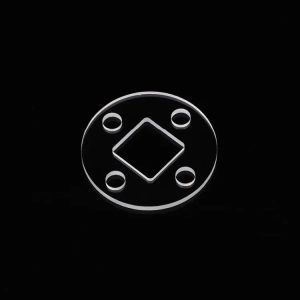
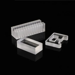
4 Specialized Quartz Window Plates
-
Freeform surfaces, asymmetric apertures, graded thickness.
-
Angled-cut windows to minimize reflection losses.
-
Through-hole windows for multi-sensor integration.
-
Rapid prototyping: 3–5 days for samples, <500-unit small batches, optional vacuum coatings (AR or reflective coatings) for research and military applications.
FAQ
1 Why choose 2-inch quartz wafers ?
2-inch quartz wafers are semiconductor-grade substrates made from high-purity silicon dioxide (SiO₂). They achieve micron-level flatness using precision CNC cutting and laser polishing. These wafers support customization in dimensions and thickness (±0.02 mm) and comply with SEMI standards, making them ideal for optoelectronics, MEMS, and semiconductor packaging.
2 What are the primary applications of 2-inch quartz wafers ?
They are primarily used in semiconductor manufacturing (CMOS image sensors, RFID chip packaging), UV laser windows, fiber-optic communication couplers, and aerospace optical components. Custom surface treatments such as Anti-Reflective coatings enhance performance in high-precision systems.

Avis
Il n’y a pas encore d’avis.