1. Johdanto
Kaksipuolinen kiillotus (DSP) on sulatetusta piilasista valmistettujen lasilevyjen mekaanisen käsittelyn viimeinen ja kriittisin vaihe. Se on myös käsittelyprosessin pisin vaihe, ja sillä on ratkaiseva merkitys lopputuotteen laadun kannalta.
Tämän prosessin aikana yleisiä pintavikoja ovat kuopat, naarmut, reunojen lohkeilut, halkeamat ja piikiekon täydellinen murtuminen. Näistä kuopat ja naarmut voidaan usein minimoida tai jopa korjata prosessin optimoinnin ja ympäristöolosuhteiden hallinnan avulla. Reunojen lohkeilut, halkeamat ja murtuminen ovat kuitenkin peruuttamattomia vikoja, jotka johtavat suoraan piikiekon hylkäämiseen.
Erittäin ohuiden sulatetun piidioksidin kiekkojen osalta murtumista johtuvat viat ovat edelleen suurin haaste korkean tuotantotehokkuuden ja vakaan tuotannon saavuttamisessa.
2. Murtumavikojen tyypit
Murtumavauriot lasilevyt ne jakautuvat yleensä kolmeen luokkaan:
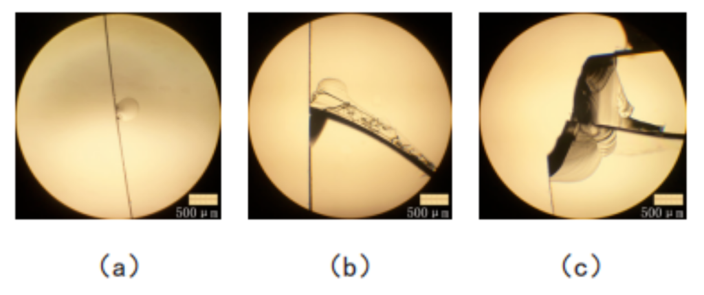
- Reunan lohkeilu (reunan murtuminen)
Määritellään yleensä näkyviksi reunavaurioiksi tai puuttuviksi palasiksi, joiden pituus on yli 0,3 mm. - Halkeaman eteneminen
Halkeamat alkavat usein lohkeilleista reunoista ja leviävät vähitellen piikiekkoon. - Täydellinen murtuma (katkeaminen)
Jos halkeamat leviävät rasituksen vaikutuksesta jatkokäsittelyn tai käsittelyn aikana, seurauksena on piikiekon katastrofaalinen vikaantuminen.
Teollisuudessa piikiekko luokitellaan yleensä vialliseksi tuotteeksi ja poistetaan jatkokäsittelystä heti, kun sen reunan lohkeilua havaitaan, sillä sen vikaantumisriski on suuri myöhemmissä vaiheissa.
3. Murtuman synty kaksipuolisen kiillotuksen aikana
DSP-prosessin aikana piikiekko on monimutkaisessa liiketilassa, jota ohjaavat seuraavat tekijät:
- Ylälevyn kierto
- Alemman levyn kierto
- Aurinkopyörän pyöriminen
- Kantajan (planeettapyörän) liike
Näissä olosuhteissa kiekkoon kohdistuu sekä kiertoliike että oma pyörimisliike, mikä tekee tarkasta jännitysanalyysistä erittäin monimutkaista.
Tuotantotilastot osoittavat kuitenkin selkeän suuntauksen: murtumaviat alkavat lähes aina piikiekon reunasta. Tämä viittaa siihen, että piikiekon reunan lujuus on murtumiskäyttäytymistä määräävä tekijä.
4. Reunan lujuus keskeisenä murtumistekijänä
Fuusioidun piikiekkojen murtumiskestävyys määräytyy pääasiassa sen reunan lujuuden perusteella.
Mekaanisen vakauden parantamiseksi kiekot käsitellään yleensä reunan viistoaminen (viistokärki), mikä auttaa vähentämään jännityskeskittymää reunoilla. Oikein suunniteltu viiste parantaa murtumiskestävyyttä merkittävästi.
Vaikka reuna olisi suojattu, virheelliset käsittelyparametrit tai liiallinen mekaaninen kuormitus voivat kuitenkin edelleen johtaa vaurion syntymiseen viistetyllä alueella.
5. Piikiekon reunan jännitysanalyysi
DSP-prosessin aikana piikiekon reunaan kohdistuu useita voimia:
- F₁: Pystysuuntainen painovoima
Syynä on pääasiassa ylälevyn kiillotuspaine. - F₂: Vaakasuora voima
Johtuu pääasiassa pyörimisen aikana syntyvistä keskipakovoimista sekä kantajajärjestelmän aiheuttamasta vastavoimasta.
Viistoreunassa nämä voimat voidaan jakaa seuraavasti:
- Viistepintaan kohtisuorat normaalivoimat
- Viistopintaan nähden yhdensuuntaiset sivuvoimat
Yhdistetty jännitystila voidaan ilmaista seuraavien tekijöiden superpositioina:
- Normaali jännitys (puristus- ja vetokomponentit)
- Leikkausjännitys (liukukomponentit)
Kun nämä jännitykset ylittävät sulatetun piidioksidin mekaanisen lujuusrajan, syntyy halkeama, joka alkaa tyypillisesti reunasta ja etenee sisäänpäin.
6. Erittäin ohuiden piikiekkojen vikaantumismekanismi
Erittäin ohuiden sulatetun piidioksidin kiekkojen (tyypillisesti paksuus < 0,3 mm) murtumisriski kasvaa merkittävästi useiden tekijöiden vuoksi:
6.1 Rakenteellisen lujuuden heikkeneminen
Paksuuden pienentyessä kiekon yleinen mekaaninen jäykkyys heikkenee merkittävästi, minkä vuoksi se reagoi herkämmin ulkoisiin rasituksiin.
6.2 Pienennetty viisteen suojausalue
Erittäin ohuilla kiekkoilla viisteen tilavuus ja kosketuspinta-ala ovat huomattavasti pienemmät. Tämän seurauksena reunan viisteen suojaava vaikutus heikkenee.
6.3 Stressikeskittymän kasvu
Samoissa kiillotusolosuhteissa:
- Kosketuspinta-ala pienenee
- Pinta-alayksikköä kohti laskettu paikallinen jännitys kasvaa
- Reunan jännityskeskittymä kasvaa huomattavasti
Tämä johtaa sekä normaali- että leikkausjännityksen nopeaan kasvuun reunalla.
7. Päätelmät
Kaksipuolisen kiillotuksen aikana sulatetusta piidioksidilasista valmistettuihin kiekkoihin syntyvät murtumaviat johtuvat pääasiassa kiekkojen reunoihin kohdistuvasta liiallisesta jännityksestä. Kun normaali- ja leikkausjännitysten summa ylittää materiaalin mekaanisen lujuusrajan, seurauksena on reunan lohkeilu, halkeaman eteneminen ja lopulta murtuminen.
Erittäin ohuet kiekot ovat erityisen haavoittuvia niiden vähäisen paksuuden, heikentyneen reunasuojauksen ja lisääntyneen jännityskeskittymän vuoksi.
Siksi piikiekkojen tuotantotehokkuuden parantaminen edellyttää erityistä huomiota seuraaviin seikkoihin:
- Reunan lujuuden optimointi
- Viisteen muotoilun parantaminen
- Kiillotuspaineen säätö
- Pyörimisnopeuden optimointi
- Prosessin vakauden parantaminen
Hallitsemalla näitä tekijöitä huolellisesti voidaan murtumariskiä vähentää merkittävästi, mikä johtaa suurempaan saantoon ja parempaan valmistusvarmuuteen sulatetun piidioksidilevyn tuotannossa.