
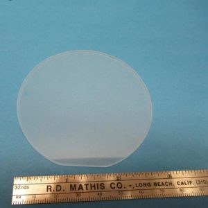
High Borosilicate Glass Wafers (3.3)
High borosilicate glass wafers are precision-engineered substrates widely used in semiconductor, MEMS, and optical applications. Known for their low thermal expansion coefficient (~3.3 × 10⁻⁶/K), excellent chemical stability, and high transparency, these wafers provide a reliable and cost-effective alternative to materials such as fused silica and quartz in medium-temperature environments.
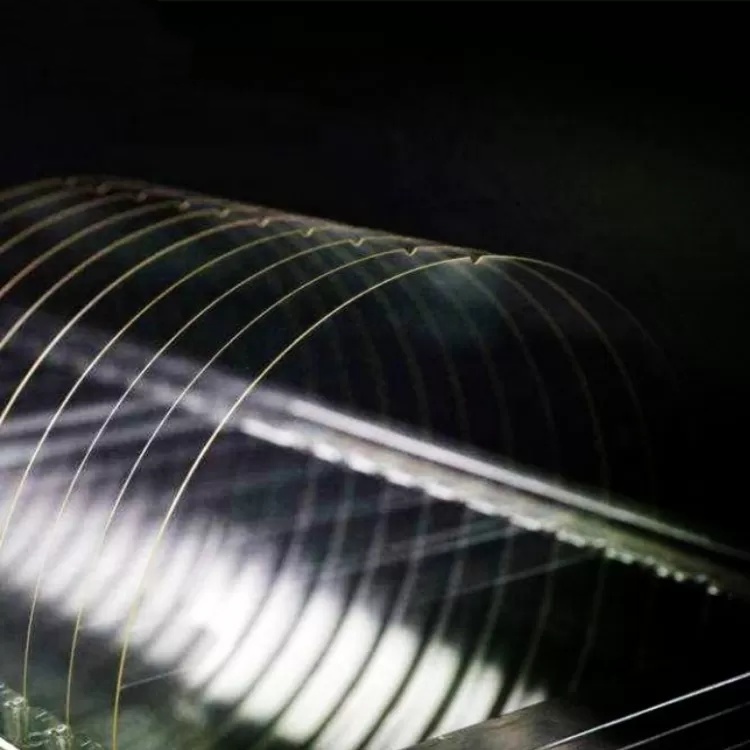
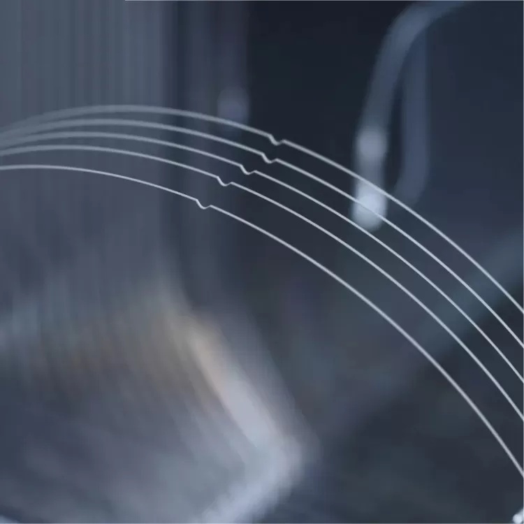
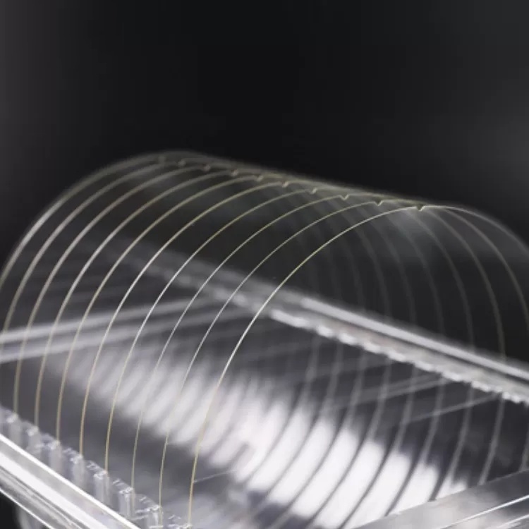
Manufactured using the float glass process, borosilicate wafers offer uniform thickness, superior flatness, and low internal stress, making them ideal for high-precision microfabrication and bonding processes.
Key Material Composition
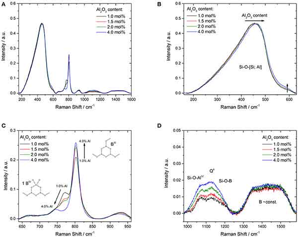
High borosilicate glass typically consists of:
- Silicon dioxide (SiO₂): ~75–80%
- Boron trioxide (B₂O₃): ~12–15%
- Aluminum oxide (Al₂O₃): small percentage
- Low alkali metal oxides (<5%)
This optimized composition provides enhanced thermal stability and chemical resistance compared to conventional soda-lime glass.
Key Advantages
Borosilicate glass wafers offer several performance benefits:
- Low thermal expansion – ideal for silicon bonding and MEMS structures
- Excellent thermal shock resistance – ΔT up to ~120–150°C (depending on thickness)
- High optical transparency – suitable for optical and photonic applications
- Strong chemical resistance – resistant to acids and most chemicals
- High flatness and surface quality – supports micro- and nano-scale fabrication
- Cost-effective – more economical than quartz or fused silica for many applications
Manufacturing Process
Borosilicate wafers are produced using the float glass method, where molten glass flows over a molten tin bath to form a smooth, uniform sheet. The material is then:
- Gradually cooled (annealed) to eliminate internal stress
- Cut into specified wafer dimensions
- Precision ground and polished (single-side or double-side)
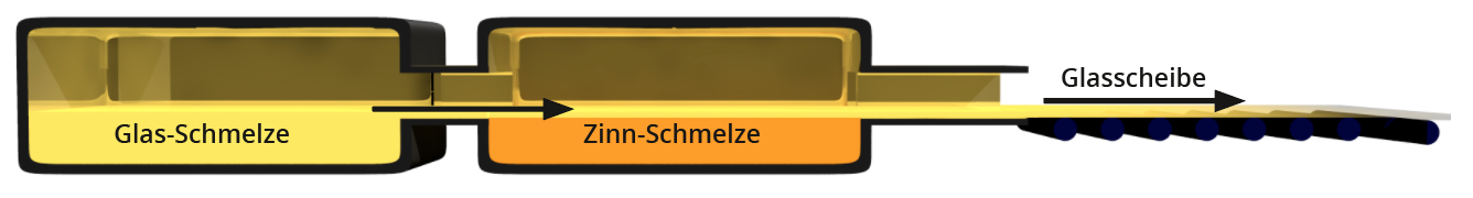
This process ensures excellent surface quality, tight thickness control, and low defect density.
Specifications
| Parameter | Range / Options |
|---|---|
| Diameter | 2” – 12” |
| Thickness | 0.2 – 1.1 mm (custom available) |
| Surface | SSP / DSP |
| Roughness | Ra < 1.5 nm |
| Flatness (TTV) | < 10 µm (typical) |
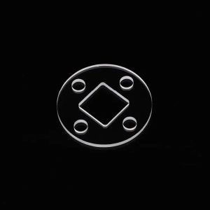
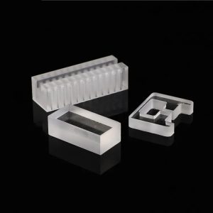
| Shape | Round / Square / Custom |
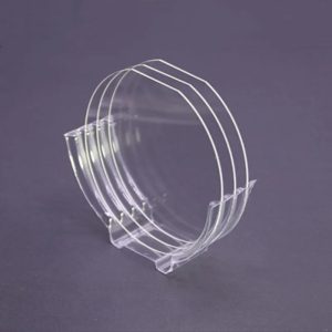
Typical Applications
1. Semiconductor & MEMS
- Wafer bonding with silicon (anodic bonding)
- MEMS devices and micro sensors
- IC packaging substrates
2. Microfluidics & Biotechnology
- Lab-on-chip devices
- Microfluidic channels
- Biomedical analysis platforms
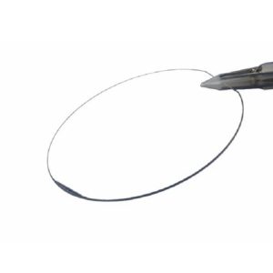
3. Optical & Photonic Systems
- Optical windows and substrates
- Lens and prism components
- Transparent carrier wafers
4. Industrial & Scientific Equipment
- High-temperature observation windows
- Laboratory equipment and analytical devices
Comparison: Borosilicate vs Soda-Lime Glass
| Property | Borosilicate Glass | Soda-Lime Glass |
|---|---|---|
| Thermal Expansion | Low (~3.3×10⁻⁶/K) | High |
| Thermal Shock Resistance | Excellent | Poor |
| Chemical Resistance | High | Moderate |
| Cost | Medium | Low |
| Applications | MEMS, optics, lab | Bottles, windows |
Why Choose Our Borosilicate Glass Wafers
- Stable supply from leading glass manufacturers
- Precision machining and polishing capabilities
- Custom sizes, thickness, and surface finishes available
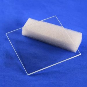
- Strict quality control and cleanroom packaging (Class 100 / ISO 5)
- Fast delivery for standard specifications
FAQ
 Q1: What is 3.3 borosilicate glass?
A: It refers to borosilicate glass with a thermal expansion coefficient of approximately 3.3 × 10⁻⁶/K, known for excellent thermal stability.
Q2: Can borosilicate glass wafers replace quartz wafers?
A: They can serve as a cost-effective alternative in medium-temperature applications, but quartz is still preferred for extreme high-temperature environments.
Q3: What is the difference between borosilicate glass wafers and quartz wafers?
A: Borosilicate glass wafers offer a more cost-effective solution with good thermal stability and chemical resistance, making them ideal for MEMS and general semiconductor applications. Quartz wafers, on the other hand, provide superior high-temperature resistance and UV transmission, and are preferred for extreme environments and advanced optical systems.
Q4: Can borosilicate glass wafers be used for anodic bonding with silicon?
A: Yes, 3.3 borosilicate glass wafers are widely used for anodic bonding with silicon due to their closely matched thermal expansion coefficient. This ensures strong bonding strength and minimizes thermal stress in MEMS and microfluidic device fabrication.
Q5: What customization options are available for borosilicate glass wafers?
A: We offer a wide range of customization options, including wafer diameter (2”–12”), thickness, single-side or double-side polishing (SSP/DSP), surface roughness, flatness (TTV), and custom shapes such as square or rectangular substrates. Special requirements for coating, drilling, or patterning can also be supported upon request.
Reviews
There are no reviews yet.