
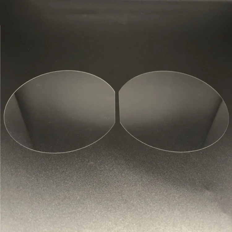

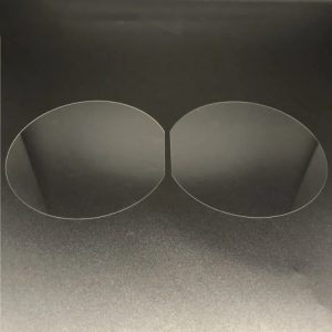
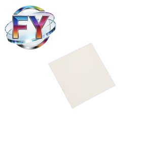
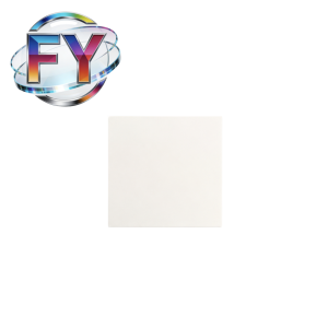
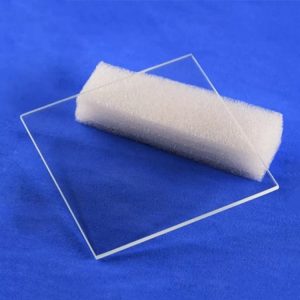
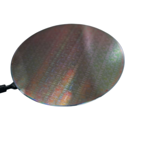
FUYAO QUARTZ 4-inch HPSI silicon carbide (SiC) wafers are high-purity, semi-insulating substrates engineered for next-generation high-performance electronic devices. Silicon carbide, a compound of silicon and carbon, provides superior electrical, thermal, and mechanical properties compared to conventional silicon wafers.
 HPSI SiC wafers are widely used in:
-
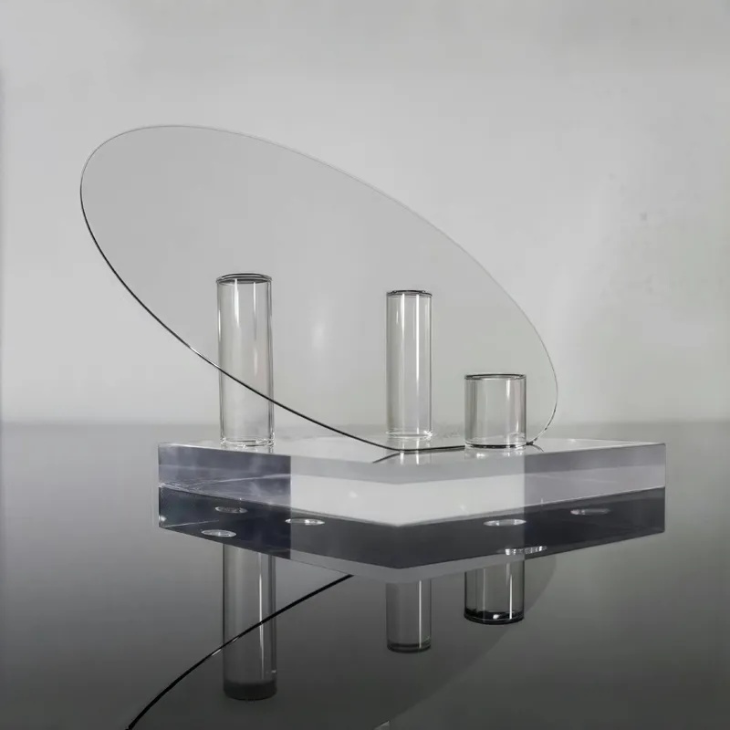
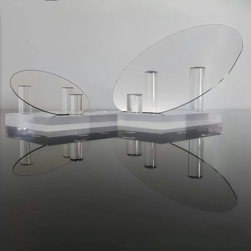
AR Glasses and Optoelectronics: Transparent SiC supports optical components with minimal energy loss.
-
High-Power Electronics: Ideal for inverters, power devices, and high-voltage applications.
-
RF and Microwave Devices: Supports high-frequency operations, including 5G communications and radar.
-
Extreme Environment Applications: Aerospace, automotive, military, and oil exploration where high temperature, high voltage, and radiation resistance are required.
The semi-insulating nature of HPSI SiC ensures low parasitic conduction, enhancing device performance and reliability in power and RF applications.
Key Advantages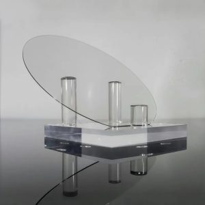
-
Wide Bandgap (~3.2 eV): Enables high breakdown voltage, low leakage, and efficient energy conversion.
-
High Thermal Conductivity: Efficient heat dissipation for high-power applications.
-
High Breakdown Electric Field: Supports high-voltage device fabrication without material degradation.
-
High Electron Mobility: Fast switching speeds for RF and power devices.
-
Chemical and Mechanical Stability: Resistant to high temperatures, voltages, frequencies, and radiation, suitable for harsh environments.
Technical Specifications
| Parameter | Specification |
|---|---|
| Crystal Material | High-Purity Single-Crystal SiC |
| Type | HPSI (Semi-Insulating) |
| Diameter | 100 ± 0.5 mm (4 inch) |
| Thickness | 350 μm ± 15 μm (4H-N), 500 μm ± 15 μm (4H-SI) |
| Wafer Orientation | Off-axis 4° toward <11-20> (4H-N), On-axis <0001> ±0.5° (4H-SI) |
| Resistivity | 4H-N: 0.015–0.024 Ω·cm; 4H-SI: ≥1×10¹⁰ Ω·cm |
| Primary Flat Orientation | {10-10} ±5° |
| Primary Flat Length | 32.5 ± 2 mm |
| Secondary Flat Orientation | Silicon face up, 90° CW from primary flat ±5° |
| Edge Exclusion | 3 mm |
| Total Thickness Variation (TTV) / Bow / Warp | ≤5 μm / ≤15 μm / ≤30 μm (4H-N) ; ≤15 μm / ≤25 μm / ≤40 μm (4H-SI) |
| Surface Roughness | Polished Ra ≤ 1 nm; CMP Ra ≤ 0.2 nm |
| Edge & Surface Defects | No significant scratches; edge chips ≤1 mm (≤5 allowed per wafer) |
| Packaging | Multi-wafer cassette or single wafer container, vacuum sealed |
Applications
-
Augmented Reality (AR) Glasses: Transparent HPSI SiC wafers for optical and electronic integration.
-
Power Electronics: High-voltage inverters, converters, and energy-efficient devices.
-
RF & Microwave Devices: Next-generation wireless communications, radar, and satellite components.
-
Harsh Environment Electronics: Aerospace, automotive, military, and oil exploration.
-
Strategic Industries: Solar energy, semiconductor lighting, smart grids—reducing energy consumption and device size.
 Quality Assurance
FUYAO QUARTZ implements strict quality control including:
-
Dimensional verification and parallelism checks
-
Electrical resistivity measurement
-
Surface roughness and defect inspection
-
Compliance with RoHS and international industry standards
These processes ensure high reliability and performance for high-power, high-frequency, and high-temperature applications.
FAQ
Q: What is a HPSI SiC wafer?
A: HPSI (High-Purity Semi-Insulating) SiC wafers are semiconductor substrates with very high resistivity, ideal for high-voltage, high-frequency, and optoelectronic applications.
Q: How does SiC differ from conventional silicon wafers?
A: Silicon wafers are low-cost and suitable for standard low-power electronics, whereas SiC wafers are next-generation substrates capable of operating under high voltage, high power, high temperature, and high-frequency conditions.
Q: What industries use SiC wafers?
A: Power electronics, RF/microwave devices, optoelectronics (AR glasses), aerospace, automotive, military, and energy applications.

Reviews
There are no reviews yet.