
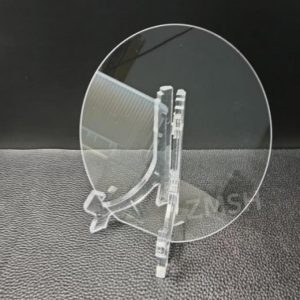
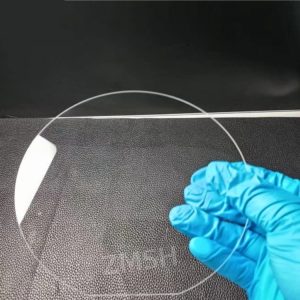
Product Overview
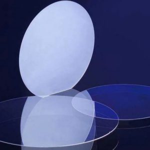
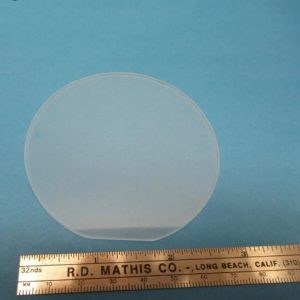
JGS1 and JGS2 quartz wafers are high purity fused silica substrates mainly composed of silicon dioxide (SiO₂). These optical grade quartz wafers are widely used in semiconductor manufacturing, ultraviolet optical systems, laser equipment, and fiber optic communication devices.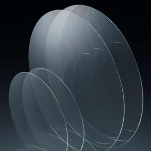
JGS1 quartz wafers are produced using the chemical vapor deposition process. This manufacturing method provides extremely low metallic impurity levels and very low hydroxyl content, allowing excellent transmission performance in the deep ultraviolet region.
JGS2 quartz wafers are typically manufactured using the hydrogen oxygen flame fusion process. Compared with JGS1, JGS2 contains higher hydroxyl content but provides stable optical performance across the ultraviolet to near infrared spectrum while maintaining a more cost effective manufacturing process.
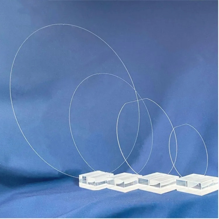
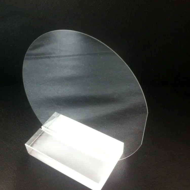
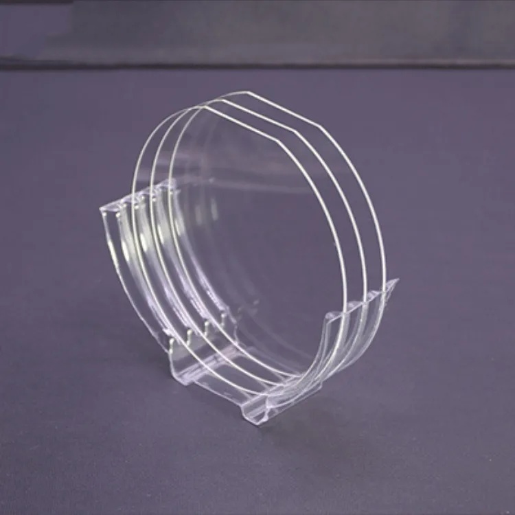
Quartz wafers are available in diameters from 2 inches to 12 inches and can be customized according to thickness, surface polishing requirements, and optical specifications.
JGS1 and JGS2 Quartz Wafer Comparison
| Property | JGS1 Quartz | JGS2 Quartz |
|---|---|---|
| Manufacturing Method | Chemical Vapor Deposition | Hydrogen Oxygen Flame Fusion |
| Optical Transmission Range | 185 nm to 2500 nm | 220 nm to 2500 nm |
| Transmittance | >85 percent at 185 nm (10 mm thickness) | >80 percent at 220 nm (10 mm thickness) |
| Metallic Impurity Content | Approximately 0.1 ppm | Approximately 1 ppm |
| Hydroxyl Content | Less than 5 ppm | 30 to 50 ppm |
| Internal Defects | Very few bubbles and streaks | Possible small bubbles or granular structures |
| Optical Homogeneity | Very high | Good |
| Thermal Stability | Good | Higher thermal stability |
Physical and Mechanical Properties
| Property | Value |
|---|---|
| Density | 2.2 g/cm³ |
| Mohs Hardness | 6 to 7 |
| Compressive Strength | 1100 MPa |
| Tensile Strength | 50 MPa |
| Bending Strength | 65 MPa |
| Torsional Strength | 30 MPa |
| Young’s Modulus | 7.5 × 10⁴ MPa |
| Poisson Ratio | 0.17 |
Electrical Properties
| Property | Value |
|---|---|
| Dielectric Constant (10 GHz) | 3.74 |
| Loss Factor (10 GHz) | 0.0002 |
| Dielectric Strength | 3.7 × 10⁷ V/m |
| Resistivity at 20°C | 1 × 10²⁰ Ω·m |
| Resistivity at 1000°C | 1 × 10⁸ Ω·m |
Thermal Properties
| Property | Value |
|---|---|
| Strain Point | 1080°C |
| Annealing Point | 1180°C |
| Softening Point | 1630°C |
| Thermal Conductivity (20°C) | 1.4 W/m·K |
| Specific Heat (20°C) | 670 J/kg·K |
| Thermal Expansion Coefficient (30°C to 600°C) | 5.5 × 10⁻⁷ /°C |
Typical Applications
| Application Field | Description |
|---|---|
| Semiconductor Lithography | Optical components and wafer processing equipment |
| Fiber Optic Communication | Optical connectors, optical windows, isolator components |
| UV Laser Systems | Excimer laser windows and optical lenses |
| Industrial UV Processing | UV sterilization equipment and high pressure mercury lamps |
| Optical Instruments | Lenses, prisms, mirrors, and optical substrates |
FAQ
 1 Difference between JGS1 and JGS2 quartz wafers ?
JGS1 quartz wafers provide higher deep ultraviolet transmission because of extremely low metallic impurities and hydroxyl content. JGS2 quartz wafers offer stable ultraviolet to near infrared performance and are generally more cost effective for standard optical applications.
2 Typical applications of JGS1 quartz wafers ?
JGS1 quartz wafers are commonly used in deep ultraviolet lithography systems, excimer laser optical components, and high precision ultraviolet optical equipment.
3 Typical applications of JGS2 quartz wafers ?
JGS2 quartz wafers are widely used in fiber optic communication devices, ultraviolet processing equipment, and general optical components that require stable UV to near infrared transmission.
Reviews
There are no reviews yet.