In the semiconductor industry, material selection is a critical factor that determines device performance, reliability, and manufacturing efficiency. Among the many materials used, quartz (SiO₂) and silicon (Si) play fundamental but distinct roles. Understanding their properties, advantages, and limitations is essential for engineers, researchers, and manufacturers aiming to optimize semiconductor processes.
1. Overview of Quartz and Silicon
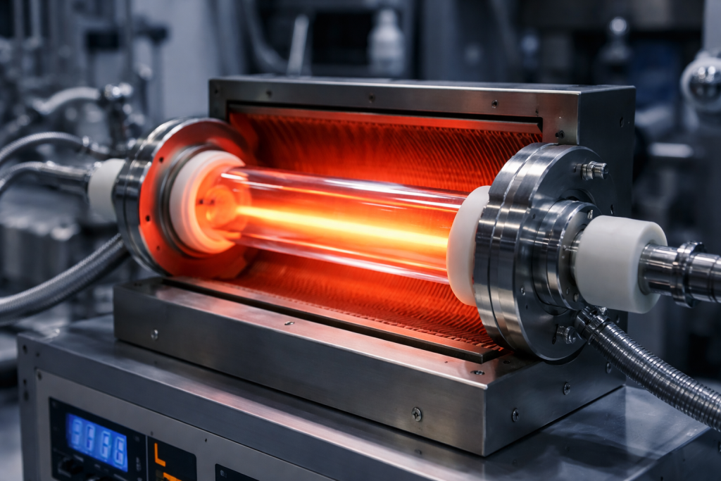
Quartz is a crystalline form of silicon dioxide (SiO₂) known for its exceptional chemical stability, high thermal resistance, and excellent dielectric properties. It is widely used in semiconductor equipment, including quartz tubes, windows, crucibles, and substrates for high-temperature processes. Its ability to withstand extreme thermal cycles without deformation makes it indispensable in processes such as chemical vapor deposition (CVD) and crystal growth.
Silicon, on the other hand, is a semiconducting material with a well-defined crystalline lattice, forming the backbone of modern microelectronics. Silicon wafers serve as the substrate upon which integrated circuits (ICs) are fabricated. Silicon’s semiconducting properties allow precise control over electron flow, enabling the creation of transistors, diodes, and logic gates that power modern computing, communication, and consumer electronics.
2. Thermal and Mechanical Properties
One of the main considerations in material selection is thermal stability. Quartz exhibits an extremely low coefficient of thermal expansion, making it highly resistant to cracking or warping during high-temperature operations, such as wafer annealing and thin-film deposition. Its melting point exceeds 1,600°C, far higher than most metals used in semiconductor tooling.
Silicon also has excellent thermal properties, with a melting point around 1,414°C, but it is mechanically more brittle under stress at high temperatures. This necessitates careful handling during wafer fabrication and processing. Quartz is therefore preferred for high-temperature environments and protective components, while silicon remains essential as the functional semiconducting substrate.
3. Chemical Resistance and Purity
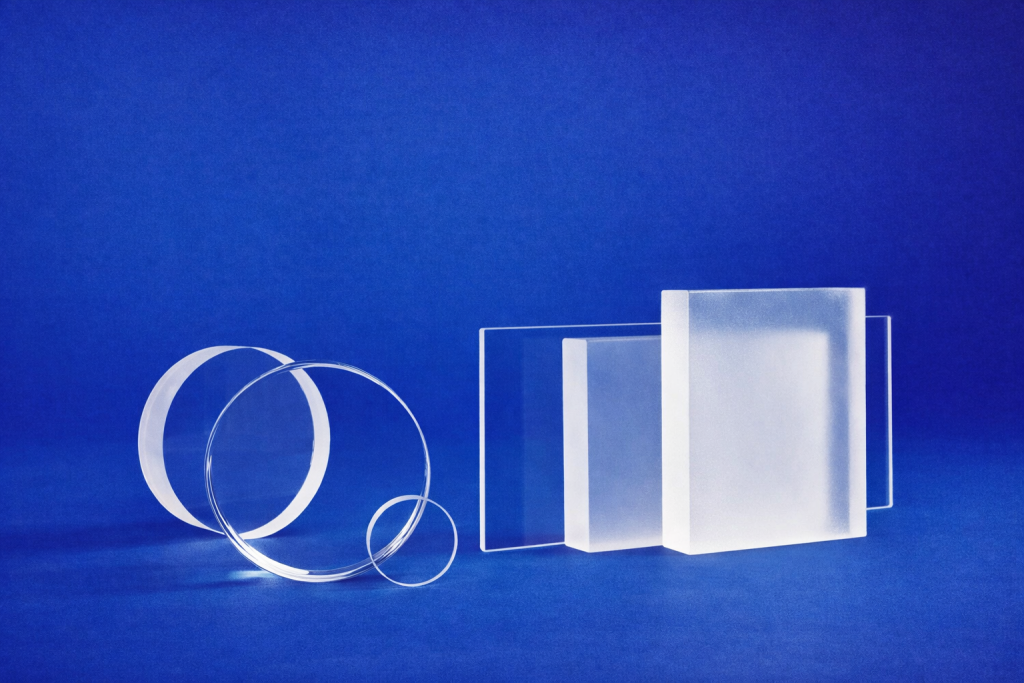
Chemical stability is another critical factor. Quartz is highly resistant to most acids and corrosive gases, making it ideal for applications such as etching chambers, process tubes, and high-purity crucibles. Impurities in quartz can affect its optical transparency and dielectric behavior, so semiconductor-grade quartz is manufactured with extremely low levels of metal contamination.
Silicon wafers require similarly stringent purity standards. Even trace impurities, such as boron or phosphorus, can significantly affect electrical characteristics. This is why silicon wafers undergo rigorous purification and doping procedures to achieve the desired electronic properties for IC fabrication.
4. Dielectric and Optical Properties
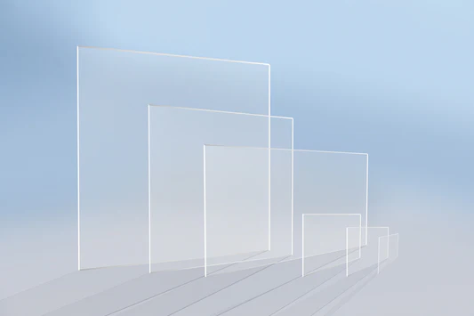
Quartz exhibits excellent dielectric strength and optical transparency, which allows it to be used in devices exposed to high-frequency signals or ultraviolet (UV) and infrared (IR) light. For example, quartz windows are used in lithography equipment and laser-assisted deposition systems to ensure stable optical transmission without introducing electrical interference.
Silicon’s dielectric properties are less critical, as its main role is to conduct and control electrical currents. However, silicon can be oxidized to form silicon dioxide (SiO₂) layers, effectively combining the semiconducting and insulating properties in a single wafer structure. This is fundamental to modern MOSFET (metal-oxide-semiconductor field-effect transistor) design.
5. Applications in Semiconductor Fabrication
Quartz applications:
- Quartz crucibles for silicon crystal growth (Czochralski process)
- Quartz tubes and reactors in CVD and thermal oxidation processes
- Quartz windows for UV and IR light in photolithography and inspection systems
- High-purity quartz substrates for specialized semiconductor sensors
Silicon applications:
- Silicon wafers as the base for ICs and MEMS devices
- Doped silicon for electronic components with precise conductivity control
- Silicon-on-insulator (SOI) wafers for high-speed and low-power applications
- Power semiconductor devices, including MOSFETs and IGBTs
6. Comparative Summary
| Property | Quartz (SiO₂) | Silicon (Si) |
|---|---|---|
| Thermal Stability | Very high (melting >1600°C) | High (melting 1414°C) |
| Mechanical Strength | Brittle but stable at high T | Brittle, sensitive to thermal stress |
| Chemical Resistance | Excellent | Moderate, requires protective layers |
| Dielectric Strength | High | Moderate, used with oxide layers |
| Optical Properties | Transparent to UV/IR | Opaque, mainly for semiconductor conduction |
| Primary Role | Equipment, substrates, insulation | Functional semiconductor substrate |
7. Conclusion
Both quartz and silicon are indispensable in semiconductor technology, but they serve fundamentally different purposes. Quartz excels as a thermally stable, chemically resistant, and optically transparent material for process equipment and high-temperature substrates. Silicon is the core functional material, providing semiconducting properties that enable modern electronics.
The choice between quartz and silicon is therefore context-dependent, determined by whether the application requires structural stability, chemical purity, optical performance, or active semiconducting functionality. Understanding these differences allows engineers and researchers to optimize processes, improve yield, and develop next-generation semiconductor devices.