Modern semiconductor manufacturing relies on materials with exceptionally high purity and stable performance under extreme process conditions. Among these materials, high-purity quartz plays a critical role in wafer fabrication equipment, thermal processing systems, diffusion furnaces, and plasma environments. Due to its excellent thermal stability, chemical resistance, optical transparency, and extremely low contamination characteristics, 高純度石英 has become one of the most important supporting materials in advanced semiconductor production.
As chip nodes continue to shrink and wafer sizes expand from 8-inch to 12-inch and beyond, the purity requirements for process materials have become increasingly stringent. Even trace levels of contamination from quartz components can negatively affect wafer yield and device performance. Understanding the material requirements and standards for semiconductor-grade quartz is therefore essential.
What Is High Purity Quartz?
High-purity quartz (HPQ) refers to quartz materials with extremely low concentrations of metallic and non-metallic impurities. In semiconductor applications, quartz products are commonly manufactured from ultra-pure fused silica produced through flame fusion or synthetic processes.
Typical impurities controlled in HPQ include:
- 鋁 (Al)
- 鐵 (Fe)
- 鈉 (Na)
- 鉀 (K)
- 鋰 (Li)
- 鈣(Ca)
- 鈦 (Ti)
For semiconductor-grade materials, total impurity levels are often measured in parts per million (ppm) or even parts per billion (ppb).
The quality of quartz directly influences contamination control inside process equipment. This is particularly important because semiconductor fabrication environments demand atomic-level precision.
Why Quartz Is Used in Semiconductor Manufacturing
Quartz possesses a unique combination of properties rarely found in other materials.
| 財產 | 高純度石英 |
|---|---|
| SiO₂ 含量 | >99.99–99.9999% |
| Maximum Working Temperature | ~1100–1250°C |
| 軟化點 | ~1730°C |
| 熱膨脹係數 | ~0.5 ×10⁻⁶/K |
| 光傳輸 | Excellent UV–IR |
| 耐化學性 | 極佳 |
| Electrical Insulation | 非常高 |
These characteristics enable quartz to function reliably in harsh semiconductor environments involving:
- High temperatures
- Rapid thermal cycling
- Reactive gases
- Plasma exposure
- Ultra-clean processing
Its low thermal expansion also minimizes dimensional changes during heating cycles.
Major Applications of High Purity Quartz in Semiconductor Equipment
Quartz components are widely used throughout wafer fabrication systems.
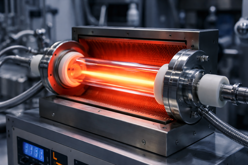
石英管
Diffusion and oxidation furnaces use quartz tubes to contain wafers during high-temperature processing. The material must withstand prolonged exposure above 1000°C while maintaining dimensional stability.
Wafer Boats and Carriers
Quartz wafer carriers support multiple wafers during thermal treatments. They require excellent mechanical integrity and contamination resistance.
Quartz Rings and Process Shields
Etching and deposition systems employ quartz rings, liners, and shields to protect chamber components from corrosive gases and plasma bombardment.
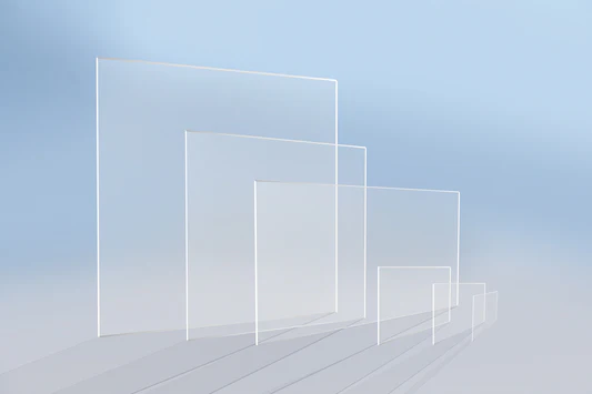
石英窗口片
Optical systems and plasma monitoring equipment utilize quartz windows due to their high transparency and thermal durability.
半導體消耗品
Many semiconductor consumables rely on precision quartz machining for process stability and repeatability.
Purity Requirements in Advanced Semiconductor Processes
As integrated circuit technologies advance toward smaller nodes, material purity standards become increasingly strict.
Typical purity classifications are shown below:
| Quartz Grade | Typical Purity |
|---|---|
| Standard Industrial Quartz | 99.9% |
| Electronic Grade Quartz | 99.99% |
| Semiconductor Grade Quartz | 99.999% |
| Synthetic Ultra-Pure Quartz | 99.9999%+ |
For advanced semiconductor production, impurity concentrations are often reduced to single-digit ppm or lower.
Particular attention is given to alkali metal contaminants because sodium and potassium ions can migrate into silicon devices and degrade electrical performance.
Contamination Challenges in Semiconductor Processing
Quartz is chemically stable, but under harsh process conditions contamination can still occur.
Common contamination sources include:
Surface Metallic Residues
Improper cleaning or machining processes may leave trace metallic particles on component surfaces.
Devitrification
Repeated thermal exposure can gradually transform amorphous quartz into crystalline structures. This process may increase particle generation and reduce transparency.
Plasma Erosion
Plasma environments can slowly erode quartz surfaces, releasing microscopic particles into process chambers.
Thermal Stress Cracking
Rapid heating and cooling cycles may introduce internal stress and cause cracking.
Because of these factors, semiconductor manufacturers impose strict inspection and qualification procedures.
Manufacturing Standards for Semiconductor Quartz Components
Producing semiconductor-grade quartz involves highly controlled manufacturing methods.
Critical processes include:
Raw Material Selection
Only ultra-high-purity silica feedstock can be used.
Precision Fusion Processing
Controlled flame fusion or synthetic deposition methods minimize contamination introduction.
CNC 加工
Precision machining ensures tight dimensional tolerances for semiconductor equipment.
Surface Polishing
Smooth surfaces reduce particle generation and improve contamination resistance.
Cleaning and Packaging
Final cleaning often involves:
- Ultra-pure water systems
- 酸洗
- Class 100 or Class 10 cleanroom environments
- Vacuum packaging
Strict particle control is essential before shipment.
High Purity Quartz vs Alternative Materials
Other advanced materials are also used in semiconductor systems.
| 材質 | 耐溫性 | 純淨 | Plasma Resistance | 典型應用 |
|---|---|---|---|---|
| 高純度石英 | 高 | 極佳 | 中度 | Furnace systems |
| Alumina Ceramics | 非常高 | 高 | 良好 | Structural components |
| Silicon Carbide | 極高 | 高 | 極佳 | Etching hardware |
| 藍寶石 | 高 | 極佳 | 中度 | 光學窗 |
Quartz remains dominant in many furnace and thermal applications due to its combination of purity, transparency, and manufacturability.
Future Trends in Semiconductor Quartz Technology
Emerging semiconductor technologies continue driving demand for improved quartz materials.
Future development areas include:
- Synthetic quartz with lower impurity concentrations
- Larger-diameter quartz components
- Enhanced plasma resistance
- Reduced particle generation
- Improved dimensional stability for advanced process nodes
As semiconductor devices become increasingly complex, the importance of material purity will continue to grow.
總結
High-purity quartz is far more than a simple supporting material in semiconductor manufacturing. It serves as a critical enabling technology that directly influences process stability, contamination control, and production yield.
As the semiconductor industry moves toward more advanced nodes and stricter manufacturing tolerances, the requirements placed on quartz materials will become increasingly demanding. Understanding purity standards, contamination mechanisms, and material selection criteria is essential for both equipment manufacturers and semiconductor process engineers.
What purity level is typically required for semiconductor quartz?
Semiconductor applications commonly require quartz purity above 99.999%, with metallic impurities controlled at ppm or ppb levels.
Why can’t ordinary industrial quartz be used in semiconductor manufacturing?
Standard industrial quartz contains higher impurity concentrations that may introduce contamination and negatively affect device performance.
What is the difference between natural and synthetic quartz?
Synthetic quartz generally offers lower impurity content and better consistency, making it suitable for advanced semiconductor processes.