
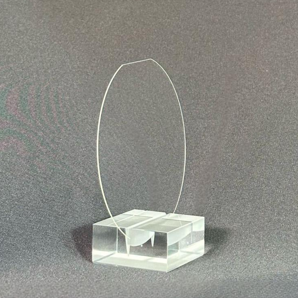

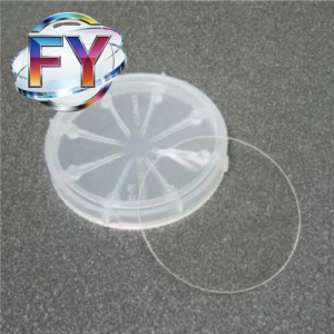
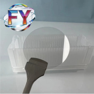
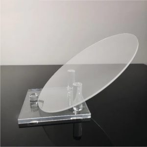
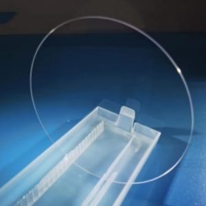
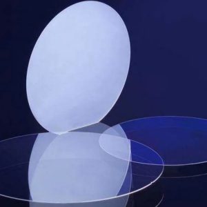
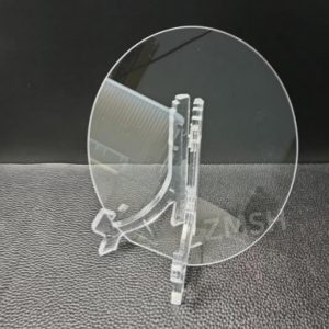
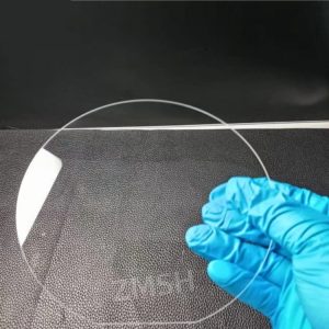
 The 4 inch high purity fused silica quartz wafer is a precision engineered optical and semiconductor substrate designed for advanced MEMS, photonic, and microelectronic applications. Manufactured from ultra-low impurity SiO₂ material, this wafer provides excellent optical transmission, outstanding thermal stability, and superior surface quality.
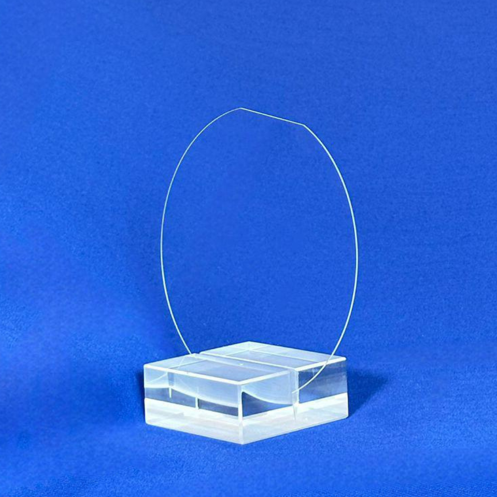
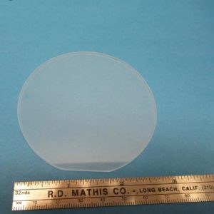
With a diameter of 100 mm, the wafer supports custom thickness ranging from 0.5 mm to 1.5 mm, making it highly flexible for different device structures and integration requirements. The double-side polished (DSP) surface ensures ultra-smooth flatness with surface roughness as low as Ra ≤ 0.5 nm, significantly reducing optical scattering and improving device accuracy.
Compared with standard glass or ceramic substrates, fused silica offers much higher thermal resistance, lower thermal expansion, and better chemical stability, making it suitable for demanding environments such as high-temperature processing, UV lithography, and precision optical systems.
 主要功能
主要功能
- Ultra-high purity fused silica (SiO₂) with extremely low metallic impurities
- Custom thickness range from 0.5 mm to 1.5 mm for flexible applications
- Double-side polished surface with Ra ≤ 0.5 nm ultra-smooth finish
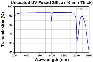
- Excellent UV to IR transmission from 185 nm to 3500 nm
- Extremely low thermal expansion coefficient (0.55 × 10⁻⁶/°C)
- High mechanical strength with Mohs hardness around 7
- Strong chemical resistance suitable for harsh process environments
技術規格
| 參數 | 價值 |
|---|---|
| 直徑 | 4 inch (100 mm) |
| 材質 | High Purity Fused Silica (SiO₂) |
| 厚度範圍 | 0.5 mm – 1.5 mm |
| 表面處理 | Double Side Polished (DSP) |
| 表面粗糙度 | Ra ≤ 0.5 nm |
| 透光率 | >92% @ 185–3500 nm |
| Thermal Expansion (CTE) | 0.55 × 10⁻⁶/°C (20–300°C) |
| 平行性 | ≤ 3 微米 |
| Resistivity (350°C) | >7 × 10⁷ Ω·cm |
材料特性
Fused silica is widely recognized as one of the most stable and high-performance optical materials available today. Its structure is composed of highly pure silicon dioxide, which provides excellent optical, thermal, and mechanical properties.
The material exhibits extremely low optical absorption across a wide spectral range, making it suitable for UV lithography, laser optics, and photonic devices. Its low thermal expansion ensures minimal deformation under temperature variations, which is critical for high-precision semiconductor processes.
In addition, fused silica offers excellent resistance to most acids and chemical environments, ensuring long-term durability in industrial and laboratory applications.
應用領域
MEMS 裝置
Used in pressure sensors, gyroscopes, inkjet systems, and micro-actuators. The wafer’s stability and precision surface quality support multi-layer microfabrication and high reliability operation.
Optoelectronic Systems
Applied in UV laser components, optical collimators, and fiber communication devices. Its high transmittance ensures low optical loss and stable signal performance.
半導體封裝
Used as wafer-level packaging substrate for CMOS sensors, RF devices, and advanced integrated circuits. Supports high-density integration and TSV structures.
Photonics and Quantum Applications
Suitable for quantum sensing, NV center research, and advanced photonic systems requiring ultra-low defect density and high optical uniformity.
Engineering Capabilities and Customization
This product supports full customization based on customer requirements, including precision machining and advanced surface treatment technologies.
Precision cutting and polishing allow dimensional accuracy within micrometer-level tolerances. Optional surface coatings such as anti-reflective (AR) coatings or hydrophobic layers can be applied to enhance optical or environmental performance.
Prototype development is available for rapid testing and evaluation, supporting complex geometries such as notches, holes, and stepped structures for specialized device integration.
常見問題
Q1 Why choose fused silica for high precision applications
Fused silica provides a unique combination of ultra-low thermal expansion, high optical transmission, and excellent chemical resistance, making it ideal for precision optical and semiconductor systems.
Q2 What is the advantage of Ra ≤ 0.5 nm surface roughness
Ultra-smooth surfaces significantly reduce light scattering and improve optical performance. This is critical in UV lithography, laser systems, and photonic devices where signal loss must be minimized.
Q3 Can thickness be customized for different applications
Yes, the wafer supports a thickness range from 0.5 mm to 1.5 mm, allowing flexibility for different mechanical strength, optical path length, and integration requirements.
商品評價
目前沒有評價。