In modern high-tech industries, optical performance is no longer just about transparency. It is about precision, stability, environmental resistance, and long-term reliability. Among advanced optical materials, fused silica (yüksek saflıkta erimiş kuvars) has become one of the most critical engineering materials used in demanding applications such as semiconductors, laser systems, aerospace optics, and scientific instrumentation.
This article provides a technical and application-oriented overview of fused silica optical components, helping engineers and procurement teams understand why this material is widely used in high-precision systems.
1. What Are Fused Silica Optical Components?
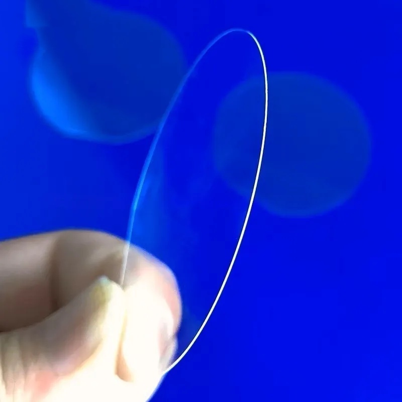
Fused silica optical components are precision parts made from ultra-high purity silicon dioxide (SiO₂). Unlike conventional glass, fused silica is manufactured by melting natural or synthetic silica at extremely high temperatures and cooling it into a non-crystalline (amorphous) structure.
This process results in a material with:
- Extremely low impurity content
- High optical transmission across UV, visible, and IR ranges
- Very low thermal expansion coefficient
- Exceptional resistance to thermal shock and chemical corrosion
Common fused silica optical components include:
- Optik pencereler
- Lenses and prisms
- Wafer carriers and substrates
- Laser system components
- UV transmission plates
- Precision inspection windows
These components are widely used in environments where standard optical glass would fail.
2. Key Material Advantages of Fused Silica
2.1 Ultra-High Optical Transmission
One of the most important properties of fused silica is its broad spectral transmission range, typically from deep ultraviolet (UV) to infrared (IR).
This makes it ideal for:
- UV lithography systems in semiconductor manufacturing
- High-power laser transmission systems
- Scientific spectroscopy instruments
Unlike standard optical glass, fused silica maintains stable transmission even under high-energy light exposure.
2.2 Extremely Low Thermal Expansion
Fused silica has a thermal expansion coefficient close to zero (~0.5 × 10⁻⁶ /K), which means:
- Minimal deformation under temperature changes
- High dimensional stability
- Excellent performance in thermal cycling environments
This property is especially critical in precision optical alignment systems, where even micrometer-level deformation can affect system accuracy.
2.3 High Chemical Resistance
Fused silica is highly resistant to most acids, salts, and chemical vapors. It performs exceptionally well in:
- Semiconductor wet etching processes
- Chemical vapor deposition (CVD) environments
- Harsh laboratory conditions
The only common chemical that significantly affects it is hydrofluoric acid (HF).
2.4 High Purity and Low Fluorescence
Due to its extremely low impurity content, fused silica exhibits:
- Minimal autofluorescence
- Low light scattering
- High signal clarity in optical systems
This makes it essential for high-end imaging, photonics, and laser measurement systems.
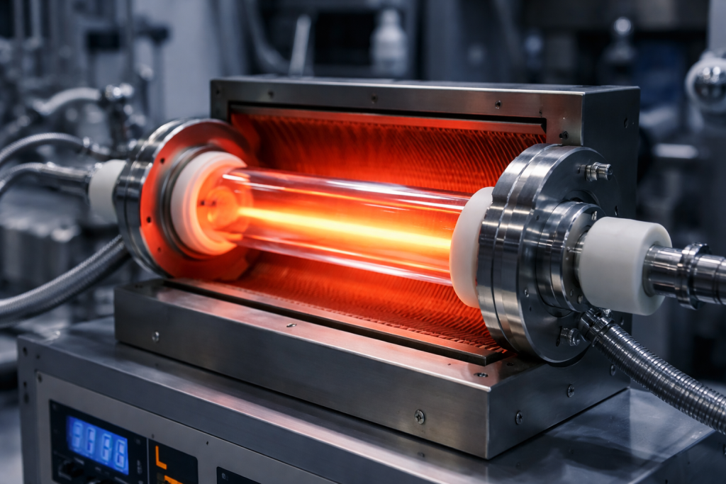
3. Manufacturing and Precision Processing
Producing fused silica optical components requires advanced manufacturing techniques.
Typical process stages include:
- Raw material purification
High-grade silica is refined to remove metallic and organic impurities. - High-temperature fusion
Silica is melted above 1700°C to form a homogeneous structure. - Precision forming
Components are shaped using CNC machining, diamond grinding, or laser cutting. - Optical polishing
Surfaces are polished to nanometer-level roughness depending on application requirements. - Inspection and metrology
Components are tested for flatness, transmission, and defect density.
Because of these strict processes, fused silica optical components are typically used in high-value engineering systems, not general-purpose applications.
4. Endüstriyel Uygulamalar
4.1 Semiconductor Industry
Fused silica is widely used in semiconductor manufacturing for:
- Wafer carriers
- Photomask substrates
- UV lithography windows
- Etching chamber components
Its stability under high temperature and corrosive gases makes it indispensable in cleanroom environments.
4.2 Laser and Photonics Systems
In laser applications, fused silica is used for:
- High-power laser windows
- Beam steering optics
- Q-switch components
- UV laser transmission plates
Its ability to handle high energy density without degradation is a key advantage.
4.3 Aerospace and Defense
Fused silica components are used in:
- Satellite optical systems
- Navigation sensors
- High-altitude observation systems
These environments require materials that can withstand extreme temperature fluctuations and radiation exposure.
4.4 Scientific and Laboratory Equipment
Uygulamalar şunları içerir:
- Spectroscopy cuvettes
- Precision optical benches
- UV and IR measurement systems
Fused silica ensures accurate and stable measurement results over long periods.
5. Fused Silica vs Standard Optical Glass
A simplified comparison helps clarify its advantages:
| Mülkiyet | Standard Optical Glass | Fused Silica |
|---|---|---|
| UV İletimi | Sınırlı | Mükemmel |
| Termal Kararlılık | Orta düzeyde | Çok Yüksek |
| Kimyasal Direnç | Orta | Mükemmel |
| Optik Saflık | İyi | Çok Yüksek |
| Maliyet | Düşük | Daha yüksek |
From an engineering standpoint, fused silica is not chosen for cost efficiency but for performance reliability in extreme conditions.
6. Engineering Perspective: Why Industry Prefers Fused Silica
In real-world engineering environments, material failure is not an option. Fused silica is preferred because it provides:
- Predictable long-term stability
- Minimal optical distortion under stress
- High resistance to environmental degradation
- Compatibility with ultra-clean manufacturing processes
This makes it a standard material in industries where precision directly affects yield, safety, or system performance.
7. Sonuç
Fused silica optical components represent a critical class of advanced engineering materials designed for high-precision and high-reliability applications.
Their combination of:
- Superior optical transmission
- Olağanüstü termal kararlılık
- Yüksek kimyasal direnç
- Ultra-low impurity content
makes them indispensable in semiconductor, laser, aerospace, and scientific industries.
While more expensive than conventional glass materials, their performance advantages often justify the investment in mission-critical systems.