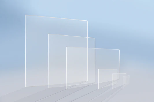
En glasskiva är ett cirkulärt substrat med hög precision, tillverkat av avancerade glasmaterial. Den tillverkas vanligtvis av material som smält kvartsglas, alkalfritt glas och kompositmaterial av glas och kisel. Genom precisionsprocesser som skärning, slipning och polering omvandlas dessa material till ultraplana skivor med strikt kvalitetskontroll av mått och yta.
Som ett nytt funktionellt material, glasplattor används i stor utsträckning inom halvledartillverkning, mikroelektronik, optisk teknik och avancerad förpackningsteknik. De har utmärkt kemisk stabilitet, hög värmebeständighet, låg ytjämnhet och hög optisk genomstrålning, vilket gör dem mycket värdefulla inom högteknologiska branscher.
I takt med den fortsatta miniatyriseringen och de ökande precisionsförbättringarna inom halvledarprocesserna blir glasplattor ett allt viktigare komplement till kiselbaserade material och visar stor potential inom mikrosystemteknik, optoelektronik och konsumentelektronik.
Definition och viktiga egenskaper hos glasplattor
Glasplattor, särskilt plattor av smält kvartsglas, är högprecisionsglasunderlag som har utvecklats parallellt med tekniken inom halvledar- och optikindustrin.
Jämfört med konventionella glasprodukter kräver glasplattor en betydligt strängare kontroll av följande:
- Måttsäkerhet
- Jämnhet i tjocklek
- Ytans planhet och ojämnhet (som ofta ligger på mikron- eller till och med nanometernivå)
Viktiga prestandafunktioner
Glasplattor uppvisar vanligtvis följande egenskaper:
- Utmärkt högtemperaturbeständighet
- Hög kemisk korrosionsbeständighet
- Hög optisk genomtränglighet
- Stabila mekaniska och elektriska egenskaper
- Extremt låg ytjämnhet
Tack vare dessa egenskaper kan glasskivor uppfylla de höga kraven som ställs på MEMS-enheter, CMOS-bildsensorer, CCD-bildsystem, mikrovågskretsar, IoT-enheter samt olika optiska komponenter och laserkomponenter.
Dessutom kan glasskivor inom optiska tillämpningar inte bara fungera som basmaterial för optiska komponenter utan även för precisionskonstruktioner såsom linser och prismor. De används också i allt större utsträckning i bärbara AR/MR-enheter och annan avancerad konsumentelektronik.
Klassificering och prestanda hos skivor av smält kvartsglas
Utifrån tillverkningsprocesser och spektrala egenskaper indelas kvartsglas i allmänhet i tre huvudtyper:
1. Syntetisk smält kvarts av UV-kvalitet (JGS1)
JGS1 tillverkas med hjälp av CVD-teknik (kemisk ångdeposition). Det har en relativt hög hydroxylhalt (cirka 950–1400 ppm) och extremt låga halter av metallföroreningar.
- Våglängdsområde: 185–2000 nm
- Egenskaper: utmärkt genomlopp för djup UV-strålning, hög strålningsbeständighet
- Användningsområden: optik för djup-UV, fotolitografisystem och avancerade optiska halvledarkomponenter
2. Flamsmält kvartsglas (JGS2)
JGS2 tillverkas med hjälp av en smältningsprocess med syre-väte-låga och har en måttlig hydroxylhalt (cirka 150–400 ppm).
- Våglängdsområde: 250–2000 nm
- Egenskaper: balanserad genomstrålning av UV-ljus och synligt ljus
- Användningsområden: allmänna optiska system, elektronikindustrin och halvledartillverkning
3. Vakuumelektrisk smältningsutrustning med infraröd kvarts (JGS3)
JGS3 tillverkas under högtemperaturvakuumförhållanden, vilket ger ett extremt lågt hydroxylinnehåll (<5 ppm).
- Våglängdsområde: 260–3500 nm
- Egenskaper: utmärkt infrarödgenomsläpplighet, lägre UV-genomsläpplighet
- Användningsområden: infraröd optik och miljöer med höga temperaturer
Glasplattors fysikaliska och kemiska egenskaper
Glasplattor har stora fördelar när det gäller både fysikaliska och kemiska egenskaper.
Elektriska egenskaper
De bibehåller hög dielektrisk hållfasthet och låg dielektrisk förlust även vid höga temperaturer, vilket gör dem lämpliga för elektroniska miljöer med hög frekvens och hög stabilitet.
Termiska egenskaper
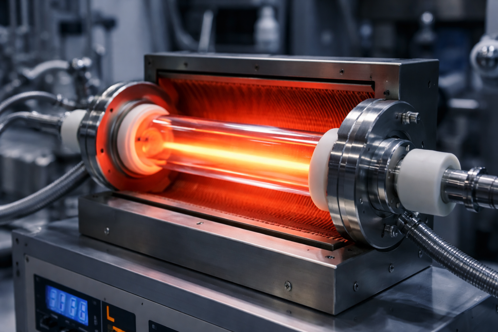
Smält kvartsglas har en extremt låg värmeutvidgningskoefficient (cirka 0,55 × 10⁻⁶/°C), med en smältpunkt på cirka 1713 °C och en mjukningspunkt nära 1580 °C. Detta garanterar utmärkt termisk stabilitet och motståndskraft mot termisk chock.
Konstruktionsstabilitet
Materialet behåller sin stabila inre struktur under komplexa bearbetningsförhållanden, vilket gör det lämpligt för långvarig användning i avancerade tillverkningsmiljöer.
Användningsområden för glasplattor inom den moderna industrin
Glasplattor spelar en avgörande roll inom flera högteknologiska branscher, framför allt inom halvledarindustrin, optik och mikroelektronik.
1. Halvledare och mikroelektronik
Inom halvledarindustrin används glasskivor i stor utsträckning inom:
- MEMS-enheter (mikroelektromekaniska system)
- CMOS-bildsensorer
- CCD-bildsystem
- Strukturer för mikrovågskretsar
- IoT-sensornätverk
De används också ofta som bärarsubstrat vid wafer-level packaging (WLP) och fan-out wafer-level packaging (FOWLP), där de ger mekaniskt stöd och stabilitet under tunnning och bearbetning av kiselskivor.
2. Optiska och optoelektroniska system
Inom traditionell optik används glasskivor i linser, prismor och laserkomponenter.
Inom modern optoelektronik används de inom:
- Optiska precisionssystem
- Högpresterande bildbehandlingsmoduler
- Sensorer och detekteringssystem
Tack vare sin höga transparens och dimensionsstabilitet är de idealiska för optiska strukturer som kräver hög precision.
3. Konsumentelektronik och nya tillämpningar
I takt med den snabba utvecklingen av AR/MR-teknik och bärbara enheter används glasplattor i allt större utsträckning inom konsumentelektroniken, bland annat:
- Optiska substrat för AR/MR
- Moduler för fingeravtrycksigenkänning
- Konstruktionskomponenter i smarttelefonkameror
- Projektions- och visningssystem
Deras utmärkta optiska klarhet och strukturella precision ger betydande fördelar i miniatyriserade optiska system.
Branschkedjans struktur
Glasplattindustrins värdekedja består av tre huvudsegment:
Uppströms
- Kvartssand med hög renhet
- Råvaror för glas
Midstream
- Smältning och formning
- Precisionsskärning
- Slipning och polering
- Avancerad kontroll och mätteknik
Nedströms
- Halvledartillverkning
- Optiska system
- Skärmtekniker
- Avancerade förpackningsindustrier
Vanliga skivstorlekar är bland annat 6-tums-, 8-tums- och 12-tumsformat, och trenden går mot större storlekar och högre precisionskrav.
Slutsats
Glasplattor är högpresterande funktionella material som förenar utmärkta termiska, optiska och kemiska egenskaper. De spelar en allt viktigare roll inom halvledar- och optoelektronikindustrin.
I takt med den ständiga utvecklingen inom mikroelektronik och optisk teknik upprätthåller glasplattor inte bara en stabil efterfrågan inom traditionella halvledartillämpningar, utan expanderar också snabbt till MEMS, AR/MR-system och avancerade förpackningsområden.
I framtiden, i takt med att tillverkningsprecisionen och materialtekniken fortsätter att förbättras, förväntas glasplattor bli ett centralt material i nästa generations avancerade tillverkningssystem.