1. Inledning
Fused silica (SiO₂) is a critical material widely used in optics, semiconductors, and high-temperature engineering due to its exceptional purity, thermal stability, and optical performance. Its manufacturing technologies can be broadly classified into two major categories: natural fused silica and synthetic fused silica.
The fundamental distinction lies in raw material sources, which subsequently determines the processing routes, impurity profiles, and final material performance.
2. Classification of Fused Silica Manufacturing Methods
2.1 Natural Fused Silica
Natural fused silica is produced by melting naturally occurring quartz crystals or silica sand, followed by rapid cooling to form an amorphous structure.
Core principle:
Direct melting of natural silica → glass formation via quenching
Depending on the heat source and process configuration, three primary methods are used:
- Electric fusion (industrial mainstream)
- Flame fusion (oxyhydrogen melting)
- Plasma melting
Key characteristics:
- Relatively low hydroxyl (OH) content
- Higher metallic impurity levels (dependent on raw material purity)
- Suitable for industrial and structural applications
2.2 Synthetic Fused Silica
Synthetic fused silica is produced from silicon-containing chemical precursors (e.g., silicon tetrachloride, silane, organosilicon compounds) through controlled chemical reactions.
Core principle:
Chemical reaction → formation of ultra-pure SiO₂ → densification
Based on reaction mechanisms, the main synthesis routes include:
- Thermal oxidation processes (dry environment oxidation)
- Kemisk förångningsdeposition med plasma (PCVD)
- Flame Hydrolysis Deposition (FHD) (most widely used)
- Sol–gel processing (wet chemical route)
Among these, FHD is the most mature and industrially dominant technology.
3. Flame Hydrolysis Deposition (FHD): Core Industrial Technology
FHD can be further divided into two distinct approaches depending on deposition and densification strategies:
3.1 Direct Deposition Method (Ingot Formation)
- High-temperature hydrolysis produces molten SiO₂ particles
- Particles are directly deposited onto a substrate
- Cooling leads to bulk fused silica ingots
Equivalent industrial concept:
- Often referred to as Kemisk förångningsdeposition (CVD) in ingot manufacturing context
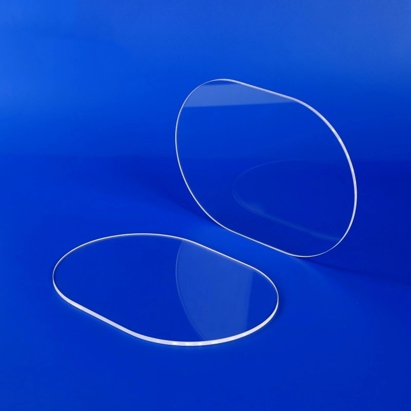
Applikationer:
- Large-size fused silica blocks
- Optical components and structural materials
3.2 Indirect Deposition Method (Soot Process)
- Low-temperature hydrolysis forms soot-like SiO₂ particles
- Particles deposit into a porous preform
- Followed by:
- Dehydration (OH removal)
- Doping (if required)
- High-temperature sintering
- Controlled cooling
Representative technologies:
- Two-step CVD process
- Vapor Axial Deposition (VAD)
- Outside Vapor Deposition (OVD)
Applikationer:
- Optical fiber preforms
- High-purity optical materials
4. Key Manufacturing Processes in Detail
4.1 Electric Fusion Method (Natural Silica Core Process)
Process steps:
- Quartz powder is heated using resistance or induction heating
- Temperature reaches ~1723 °C to form molten silica
- Melt is rapidly cooled to achieve glassy structure
During heating, quartz undergoes phase transitions:
- β-quartz → α-quartz → α-cristobalite → amorphous silica
Critical control conditions:
- High vacuum environment (0.1–10 Pa) to remove gas inclusions
- Pre-drying of raw materials to minimize moisture
Kännetecken:
- Low OH content
- Higher metallic impurities (difficult to eliminate)
4.2 Two-Step CVD Process (Improved Synthetic Route)
Background:
Traditional one-step FHD processes involve water vapor, leading to high and difficult-to-control OH content. The two-step CVD method addresses this limitation.
Step 1: Porous SiO₂ Preform Formation
- Silicon precursors (e.g., SiCl₄ or organosilicon compounds)
- React in oxyhydrogen flame
- Generate soot-like SiO₂ particles
- Deposit into a porous amorphous structure
Step 2: Sintering and Densification
- Preform transferred to high-temperature furnace
- Dehydration gas introduced to remove OH groups
- Sintering and cooling produce dense fused silica
Key advantages:
- Extremely high purity (minimal metal contamination)
- Low hydroxyl content (controllable dehydration)
- Superior performance in:
- Deep ultraviolet (DUV) transmission
- High-power laser applications
Raw material considerations:
- SiCl₄ route: mature but produces corrosive by-products (e.g., HCl)
- Organosilicon route (e.g., D4): cleaner but less industrially dominant
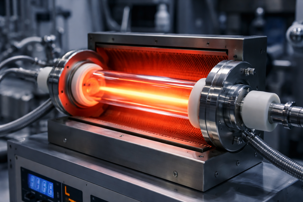
4.3 Thermal Re-Shaping Process (Post-Forming Technology)
Application:
Used to fabricate specific geometries such as:
- Quartz tubes
- Quartz rods
- Precision structural components
Process principle:
Heating stage:
- Induction heating generates electromagnetic fields
- Heat is transferred to the silica material, causing softening
Forming stage:
- Material is shaped via:
- Drawing (pulling)
- Controlled sinking or molding
Control parameters:
- Furnace temperature distribution
- Drawing speed
Quality-critical factor:
Uniform temperature field inside the furnace directly determines dimensional accuracy and structural integrity.
5. Comparative Insights: Natural vs Synthetic Fused Silica
| Aspekt | Natural Fused Silica | Synthetic Fused Silica |
|---|---|---|
| Raw material | Natural quartz | Chemical precursors |
| Renhet | Måttlig | Ultrahög |
| OH content | Låg | Controllable (can be ultra-low) |
| Metal impurities | Högre | Extremt låg |
| Kostnad | Lägre | Högre |
| Tillämpningar | Industrial, thermal | Optical, semiconductor, photonics |
6. Slutsatser
The manufacturing of fused silica has evolved from simple quartz melting techniques to highly controlled chemical synthesis processes. While natural fused silica remains important for cost-sensitive and structural applications, synthetic fused silica dominates high-end optical and semiconductor fields due to its superior purity and controllable properties.
Among all technologies, Flame Hydrolysis Deposition (FHD) and its derivative processes play a central role in modern production, especially for applications requiring:
- Ultra-low impurity levels
- Precise optical performance
- High reliability under extreme conditions
Future advancements will continue to focus on purity enhancement, defect reduction, and process stability, enabling fused silica to meet the increasing demands of next-generation photonic and semiconductor systems.