1. Введение
Fused silica, primarily composed of high-purity silicon dioxide (SiO₂), is one of the most critical materials in modern optics, photonics, and high-temperature engineering. Its exceptional combination of optical transparency, thermal stability, radiation resistance, and chemical inertness makes it indispensable across industries such as semiconductor processing, laser systems, and precision sensing.
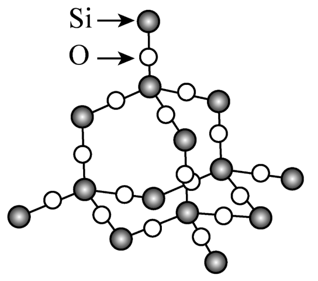
The outstanding properties of fused silica originate from its unique atomic structure, widely described by the continuous random network (CRN) model, which explains its amorphous yet highly stable configuration.
2. Atomic Structure and Fundamental Properties
In fused silica, silicon (Si) and oxygen (O) atoms form a nearly ideal three-dimensional network of Si–O tetrahedra. Each silicon atom is covalently bonded to four oxygen atoms, creating a continuous and highly interconnected structure.
Key structural characteristics include:
- High Si–O bond energy (~460 kJ/mol), ensuring strong chemical stability
- Short bond length, contributing to structural compactness
- Absence of long-range order, typical of amorphous materials but with excellent local ordering
This dense and uniform network is responsible for several critical properties:
- High optical transmission from deep ultraviolet (DUV) to infrared (IR)
- Superior resistance to radiation-induced damage
- Low thermal expansion coefficient
- Excellent chemical durability
3. Historical Development of Fused Silica Fabrication
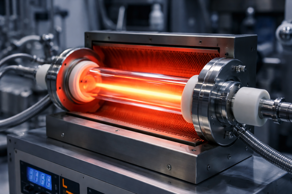
The production of fused silica dates back to the 19th century. In 1839, early experimental work using oxyhydrogen flame melting of quartz marked the first successful synthesis of fused silica glass. Since then, continuous technological advancements have significantly improved material purity, scalability, and performance.
4. Conventional Manufacturing Methods
Two industrially mature methods dominate the production of fused silica:
4.1 Electric Fusion Method
- Quartz powder is melted using electric heating
- Rapid cooling transforms the melt into amorphous glass
- Advantages: high efficiency and scalability
- Limitations: relatively higher impurity levels
4.2 Flame Fusion Method
- Natural quartz is melted using an oxyhydrogen flame
- Molten droplets are deposited layer-by-layer onto a target surface
- Produces bulk fused silica ingots
Both methods rely heavily on high-purity quartz sand, making raw material quality a critical factor in final product performance.
5. Resource Constraints and Synthetic Silica Development
High-purity quartz resources are geographically concentrated, leading to supply constraints for many manufacturing regions. This dependency has driven the development of synthetic fused silica, which offers superior purity and controllable properties.
6. Advanced Synthetic Fabrication Technologies
Modern synthetic fused silica is produced using several advanced techniques:
- Химическое осаждение из паровой фазы (CVD)
- Плазменно-химическое осаждение из паровой фазы (PCVD)
- Indirect CVD (soot deposition and sintering)
- Sol-gel processing
Among these, indirect CVD is particularly important for high-end optical applications due to its ability to:
- Minimize metallic impurities
- Reduce hydroxyl (OH) content through controlled dehydration
- Achieve excellent deep ultraviolet (DUV) transparency
- Improve laser damage resistance
7. Classification: Transparent vs. Opaque Fused Silica
Fused silica can be broadly categorized based on optical transparency:
7.1 Opaque Fused Silica
- Contains numerous microbubbles and scattering centers
- Appears translucent or opaque
- Applications: thermal reactors, crucibles, and structural components
7.2 Transparent Fused Silica
- Extremely low bubble content (often measured in ppm)
- High optical homogeneity
- Applications: precision optics, photonics, and laser systems
Transparent fused silica requires significantly stricter manufacturing conditions but delivers far superior optical performance.
8. Defect Mechanisms in Fused Silica
The performance of fused silica is closely linked to its chemical purity and structural integrity. Defects are generally classified into two categories:
8.1 Structural Defects
These arise from atomic-scale irregularities in the Si–O network:
- Metallic impurities (e.g., Fe, Cr)
- Introduce absorption losses
- Reduce optical transmission
- Hydroxyl groups (Si–OH)
- Originating from hydrogen-containing environments
- Disrupt Si–O bonding stability
- Introduce absorption bands at specific wavelengths (e.g., ~2.72 μm, 1.39 μm, 0.9 μm)
- Increase infrared attenuation
- Promote crystallization
8.2 Macroscopic Defects
These include:
- Gas bubbles
- Inclusions
- Striae (density variations)
- Cracks
Due to the high viscosity of molten silica, trapped gas bubbles are difficult to eliminate. Additionally, improper melting or cooling processes can lead to incomplete fusion or internal stress accumulation.
9. Thermal Stress and Its Optical Implications
Fused silica is a poor thermal conductor. During cooling, temperature gradients between the surface and interior generate residual thermal stress, which can severely affect optical performance:
- Refractive index variations across the material
- Optical distortion and scattering
- Stress-induced birefringence
Impact on Advanced Optical Systems:
- High-power laser systems
- Beam distortion
- Reduced stability
- Lower laser damage threshold
- Photonic devices (e.g., waveguides, filters)
- Polarization-dependent loss
- Mode distortion
- Reduced device reliability
10. Strategies for Defect and Stress Control
To ensure high-performance fused silica, advanced manufacturing processes focus on:
- Ultra-high purity precursor materials
- Controlled deposition and sintering environments
- OH content reduction (dehydration treatment)
- Precision thermal annealing to relieve internal stress
Effective stress management not only prevents cracking but also enhances:
- Optical uniformity
- Laser resistance
- Device reliability
- Manufacturing yield
11. Conclusion
Fused silica remains a cornerstone material in modern science and engineering due to its unique atomic structure and exceptional physical properties. As high-performance optical and photonic systems continue to evolve, the demand for ultra-pure, low-defect fused silica will only increase.
Advances in synthetic fabrication technologies and stress control techniques are critical to unlocking its full potential, ensuring that fused silica continues to play a vital role in next-generation industrial and scientific applications.