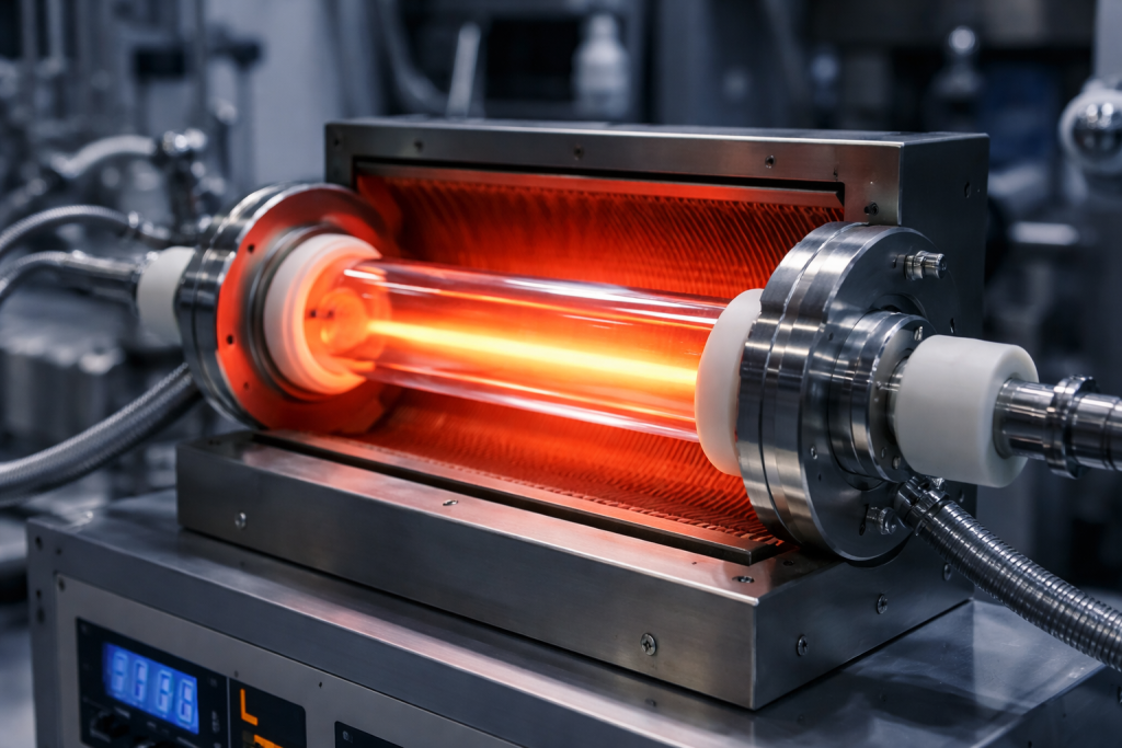
Quartz wafer carriers are widely used to hold, separate and transport semiconductor wafers during wet cleaning, chemical treatment, rinsing, oxidation, diffusion and other high-purity processing steps. Although a wafer carrier may appear to be a relatively simple component, its structural design can directly influence wafer stability, chemical circulation, particle generation, cleaning uniformity and operator handling.
A properly designed quartz wafer carrier must do more than accommodate a specified wafer diameter. It must maintain stable wafer spacing, minimize contact with critical wafer surfaces, allow process fluids to move freely and withstand repeated exposure to heat and aggressive chemicals.
This article explains the main engineering considerations involved in designing quartz wafer carriers for semiconductor cleaning and processing applications.
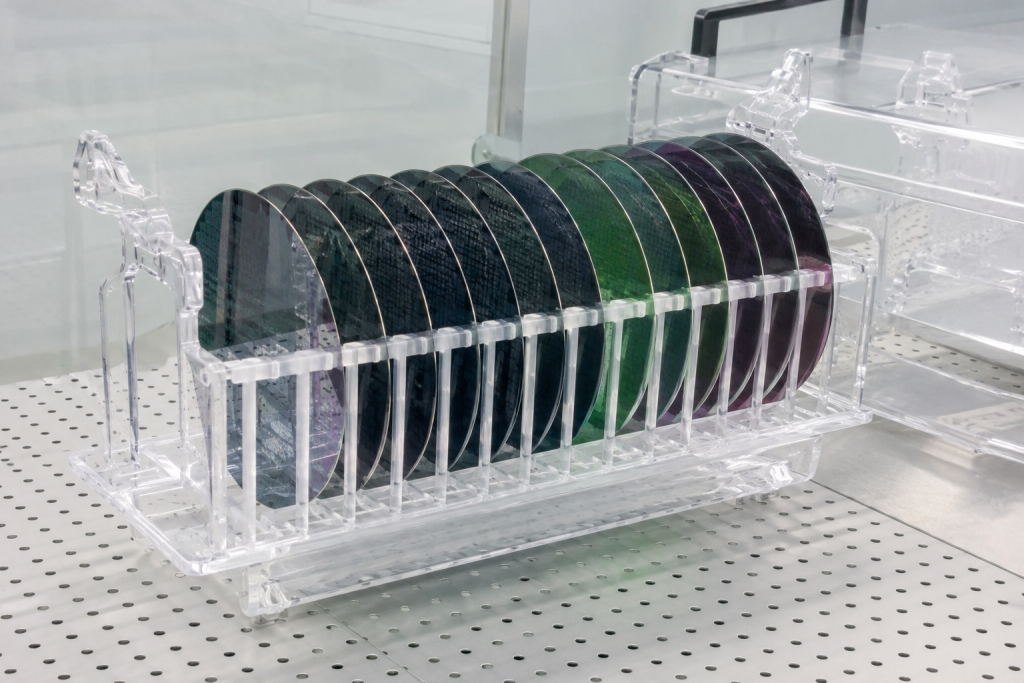
What Is a Quartz Wafer Carrier?
A quartz wafer carrier is a precision-fabricated holder designed to support multiple wafers during semiconductor manufacturing. Depending on the equipment and process, it may also be referred to as a:
- Quartz wafer boat
- Quartz cleaning carrier
- Quartz cassette
- Quartz wafer holder
- Quartz process boat
- Quartz wet bench carrier
The carrier normally contains a series of accurately spaced slots or grooves. Each slot holds one wafer while maintaining a controlled distance between adjacent wafers.
Quartz wafer carriers are commonly used in:
- RCA cleaning
- 酸洗浄
- Oxidation and diffusion preparation
- Wet etching
- DI water rinsing
- High-temperature chemical treatment
- Wafer drying
- Laboratory wafer processing
- Compound semiconductor substrate cleaning
The final carrier design depends on the wafer material, diameter, thickness, process chemistry, bath dimensions, automation system and cleanliness requirements.
Why Quartz Is Used for Wafer Carriers
High-purity fused quartz offers a useful combination of thermal stability, chemical resistance and low contamination potential.
Its coefficient of thermal expansion is much lower than that of conventional glass, helping quartz components maintain dimensional stability during temperature changes. Quartz glass also offers strong resistance to water, salt solutions and many acids, although hydrofluoric acid and some phosphoric-acid conditions can attack the material.
These characteristics make quartz suitable for semiconductor applications involving elevated temperatures, highly controlled chemical environments and strict requirements for metallic contamination.
However, material selection alone does not guarantee reliable performance. Carrier geometry, fabrication quality, surface condition and cleaning procedures are equally important.
1. Wafer Diameter and Thickness
The first design parameter is the wafer specification.
Common wafer diameters include:
- 2 inches
- 3 inches
- 4 inches
- 5 inches
- 6 inches
- 8 inches
- 12 inches
Custom carriers may also be designed for square substrates, glass wafers, sapphire wafers, silicon carbide wafers, gallium arsenide wafers and other non-standard substrates.
The designer must confirm:
- Nominal wafer diameter
- Diameter tolerance
- Wafer thickness
- Thickness tolerance
- Edge profile
- Orientation flat or notch dimensions
- Whether the wafer is rigid, thinned or unusually fragile
A carrier designed for a standard-thickness silicon wafer may not be suitable for an ultra-thin wafer. Excessive slot clearance can allow a thin wafer to tilt or move, while insufficient clearance can cause sticking, scratching or edge damage.
The slot geometry should therefore be based on the actual wafer thickness range rather than only the nominal wafer diameter.
2. Slot Width and Slot Profile
Slots are the most critical functional features of a quartz wafer carrier.
The slot width must provide sufficient clearance for wafer loading and unloading while limiting uncontrolled movement during transfer and processing.
If the slot is too narrow, it may:
- Scratch the wafer edge
- Trap the wafer during thermal expansion
- Make robotic loading difficult
- Increase the risk of breakage
- Retain chemical residue
If the slot is too wide, the wafer may:
- Lean excessively
- Vibrate during fluid movement
- Contact adjacent wafers
- Shift during transfer
- Experience uneven cleaning
Slot profiles may be rounded, V-shaped, U-shaped or specially contoured. Rounded contact areas are generally preferred because sharp internal corners can concentrate mechanical stress and are more difficult to clean.
For sensitive wafers, the carrier should contact only limited regions near the wafer edge. Critical front and back surfaces should remain as unobstructed as possible.
3. Wafer Pitch and Spacing
Wafer pitch refers to the center-to-center distance between adjacent wafer slots.
The correct pitch depends on:
- Wafer diameter
- Wafer thickness
- Chemical viscosity
- Fluid circulation
- Required batch capacity
- Megasonic or ultrasonic cleaning conditions
- Robotic handling requirements
- Drying method
A smaller pitch allows more wafers to be processed in one batch, but overly dense spacing may restrict chemical circulation and make it more difficult to remove particles from wafer surfaces.
A larger pitch improves fluid access but increases carrier length and reduces batch capacity.
The design should balance throughput with cleaning performance. In wet cleaning applications, sufficient space must be maintained so that fresh chemicals and rinse water can reach both sides of each wafer.
4. Fluid Flow and Drainage
A wafer carrier used in a chemical bath must allow process liquid to enter, circulate and drain without creating stagnant regions.
Poor drainage can result in:
- Chemical carryover
- Uneven rinsing
- Particle redeposition
- Watermarks
- Extended drying time
- Local concentration differences
Open-frame carrier designs are often preferred for wet processing because they reduce flow obstruction. Support rods, crossbars and reinforcement structures should be positioned so that they do not create unnecessary fluid shadows behind the wafers.
The bottom structure is especially important. It should support the wafers securely while allowing chemicals and rinse water to drain rapidly when the carrier is removed from the bath.
Drainage holes or open channels may be incorporated into the structure, but their edges should be properly finished to avoid particle generation and contamination traps.
5. Carrier Capacity
Quartz wafer carriers may hold only a few wafers for laboratory processing or dozens of wafers for batch production.
Higher capacity is not always better.
As carrier capacity increases:
- Overall length increases
- Mechanical loading increases
- Dimensional control becomes more difficult
- Thermal deformation risk may increase
- Manual handling becomes more difficult
- Fluid flow between wafers may become less uniform
The maximum batch size should be determined by the equipment chamber or chemical tank, transfer mechanism and required process uniformity.
For large carriers, reinforcement rods or structural supports may be required. These additions must provide mechanical stability without blocking chemical circulation.
6. Wafer Support and Contact Area
The contact area between the quartz carrier and the wafer should be carefully controlled.
Excessive contact can:
- Trap particles
- Prevent chemical access
- Create local drying marks
- Increase scratching risk
- Leave untreated regions
Insufficient support can allow the wafer to move, tilt or break.
A well-designed carrier uses a minimum number of stable contact points. These points are normally located near the wafer edge, away from active device areas.
For double-side-polished wafers or substrates with sensitive backside films, the contact geometry becomes even more important. The design should avoid broad flat contact surfaces wherever possible.
7. Orientation Flat and Notch Compatibility
Silicon and compound semiconductor wafers may include an orientation flat or notch.
The carrier design should account for:
- Flat length
- Notch position
- Required wafer orientation
- Robotic alignment method
- Process-specific orientation rules
Some cleaning carriers allow wafers to rotate freely, while others require consistent orientation. Where alignment is important, the support structure may include a positioning feature that keeps the notch or flat in a defined direction.
However, positioning features must not create excessive contact or interfere with liquid flow.
8. Mechanical Strength and Structural Stability
Quartz has excellent thermal properties, but it is a brittle material. A quartz carrier should therefore be designed to avoid concentrated mechanical stress.
Potential weak points include:
- Sharp internal corners
- Abrupt changes in cross-section
- Thin welded joints
- Unsupported long spans
- Deep narrow slots
- Uneven load distribution
Rounded transitions and balanced structures can reduce local stress. Welded joints should be smooth, properly fused and positioned away from areas subjected to repeated mechanical loading.
The carrier must also remain stable when fully loaded. A narrow base or high center of gravity can make the assembly difficult to place inside a cleaning tank.
9. Surface Finish and Edge Quality
Surface condition is critical in semiconductor processing.
Poorly finished quartz surfaces may retain contaminants or release small particles during repeated use. All edges, slots and welded regions should therefore be inspected for:
- チップス
- Microcracks
- Sharp edges
- Rough grinding marks
- Incomplete polishing
- Welding residue
- Local deformation
Flame polishing may be used on suitable areas to smooth the quartz surface, but the process must be controlled. Excessive flame treatment can alter dimensions, round precision features or introduce residual stress.
Precision slots and contact surfaces may require mechanical finishing before final cleaning.
10. Particle and Contamination Control
Quartz carriers are selected partly because of their suitability for high-purity environments. Nevertheless, particles can still originate from poor machining, handling, impact damage, chemical attack or improper cleaning.
Important contamination-control measures include:
- Using high-purity quartz raw material
- Avoiding unnecessary metal contact during fabrication
- Cleaning the carrier after machining
- Removing loose particles from slots and joints
- Using clean packaging
- Preventing direct hand contact
- Inspecting the carrier regularly during service
Carrier design should minimize hidden recesses where chemicals, particles or residues can accumulate.
Quartz is resistant to many acids, but it is not universally resistant to all semiconductor chemicals. Hydrofluoric acid directly attacks silica, and strong alkaline environments can also damage quartz under certain conditions.
The actual chemical recipe, concentration, temperature and exposure time should therefore be reviewed before finalizing the carrier material and service-life expectations.
11. Compatibility with Wet Bench Equipment
A quartz carrier must fit both the wafer and the processing equipment.
Before production, the following equipment information should be confirmed:
- Tank internal dimensions
- Maximum carrier length and width
- Bath depth
- Lifting position
- Automation interface
- Robot or transfer-arm geometry
- Guide rail dimensions
- Handle location
- Required immersion depth
- Clearance from heaters or megasonic transducers
A technically correct wafer slot design may still fail if the carrier cannot be loaded into the wet bench or picked up by the existing transfer mechanism.
For replacement carriers, physical samples, detailed drawings or precise measurements of the original component are helpful.
12. Handle and Transfer Design
The handle must support safe lifting without interfering with the process.
Manual carriers may use:
- Central lifting handles
- Side handles
- Integrated quartz hooks
- Detachable handling tools
Automated systems may require specific pickup bars, indexing features or robotic contact zones.
The handle should keep the operator’s hand away from processed wafers and chemical surfaces. It should also remain mechanically balanced when the carrier is fully loaded.
For high-temperature applications, handle length and thermal exposure should be considered.
13. Cleaning and Maintenance of Quartz Carriers
Quartz carriers should be cleaned using a procedure compatible with both the carrier and the semiconductor process.
A typical maintenance program may include:
- Visual inspection for chips and cracks
- Removal of loose particles
- Chemical cleaning using an approved process
- Thorough DI water rinsing
- Controlled drying
- Cleanroom inspection
- Clean packaging before reuse
The cleaning procedure should be established by the semiconductor facility according to its contamination-control requirements. Strong chemicals should never be selected solely because quartz is generally considered chemically resistant.
Damaged carriers should be removed from service. Small chips near wafer contact points can scratch wafers, while cracks near welded joints may lead to sudden mechanical failure.
14. Custom Quartz Carrier Manufacturing
Standard quartz carriers are suitable for common wafer sizes, but custom designs are often necessary for:
- Ultra-thin wafers
- Small research batches
- Non-standard wafer diameters
- Sapphire substrates
- SiC wafers
- Glass wafers
- Square or rectangular substrates
- Double-side-polished wafers
- Special cleaning tanks
- Automated wet benches
- High-temperature treatment systems
A custom quartz carrier project normally begins with a technical drawing or sample. The drawing should identify critical dimensions, wafer capacity, slot pitch, slot width, overall dimensions and equipment interfaces.
Where possible, tolerances should be assigned according to functional requirements. Applying unnecessarily tight tolerances to every dimension can increase manufacturing difficulty and cost without improving process performance.
Information Required When Ordering a Quartz Wafer Carrier
To prepare an accurate quotation and design review, buyers should provide:
- Wafer material
- Wafer diameter
- Wafer thickness and tolerance
- Number of wafers per carrier
- Required wafer pitch
- Slot width or available wafer clearance
- Flat or notch information
- Overall carrier dimensions
- Chemical environment
- Maximum operating temperature
- Manual or automated handling method
- Cleaning equipment dimensions
- Technical drawing, sample or reference photograph
- Cleanliness and packaging requirements
Providing complete process information at the beginning helps avoid redesign and ensures that the carrier is compatible with both the wafers and the equipment.
結論
Quartz wafer carriers play an important role in semiconductor cleaning and processing. Their performance depends on much more than wafer diameter and batch capacity.
Slot geometry, wafer pitch, support position, liquid circulation, drainage, structural strength, surface finish and equipment compatibility must all be considered together. A well-engineered carrier can improve wafer stability, reduce particle risks, promote uniform cleaning and simplify handling throughout the process.
For non-standard wafers, specialized wet benches or sensitive semiconductor processes, a custom quartz carrier designed from detailed operating requirements is usually more reliable than a generic holder.
Shanghai Fuyao Optoelectronics Tech Co., Ltd. manufactures custom quartz wafer carriers, quartz boats, quartz cleaning baskets and precision quartz components for semiconductor and laboratory processing. Products can be fabricated according to customer drawings, wafer specifications, equipment dimensions and process requirements.
What is the difference between a quartz wafer carrier and a quartz wafer boat?
The terms are sometimes used interchangeably. A wafer carrier commonly refers to a holder used for cleaning, rinsing or transport, while a wafer boat is often associated with oxidation, diffusion or furnace processing. The actual distinction depends on the equipment and manufacturer.
Can one quartz carrier be used for wafers of different thicknesses?
It may be possible when the thickness range is small and the slot clearance remains appropriate. Large thickness differences may require separate carrier designs to prevent excessive movement or loading difficulty.
Can quartz wafer carriers be used in hydrofluoric acid?
Hydrofluoric acid attacks silica and can etch quartz. The concentration, temperature and exposure time must be carefully evaluated. Alternative materials may be more suitable for prolonged HF processing.