
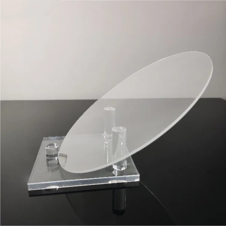
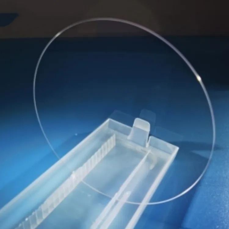
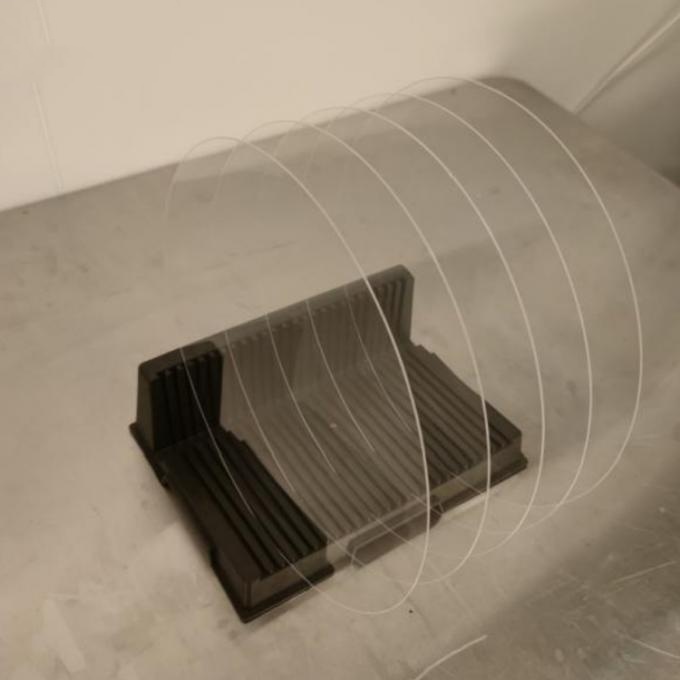
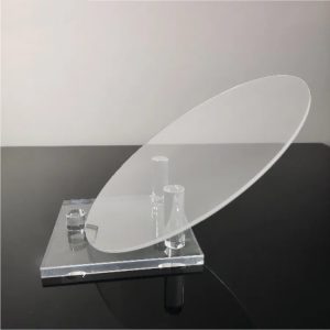
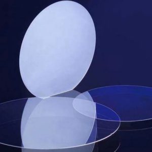
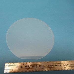
 The 8-inch fused quartz wafer is a premium high-purity synthetic quartz (SiO₂ ≥99.99%) substrate engineered for high-precision applications in semiconductor, MEMS, optical, and laser systems. Its ultra-low thermal expansion, exceptional UV-IR transmittance, and excellent chemical resistance make it ideal for demanding environments such as photolithography, etching, thin-film deposition, and high-precision sensor fabrication.
Each wafer is carefully produced under stringent quality control in a cleanroom environment to ensure superior flatness, surface finish, and purity. This guarantees reliable performance for critical industrial, research, and aerospace applications.
Key Features & Advantages
-
Ultra-High Purity (≥99.99%): Minimizes contamination in semiconductor and optical processes.
-
Exceptional Thermal Stability: Softening point ~1683°C, short-term tolerance up to 1450°C for high-temperature processes.

-
Ultra-Low Thermal Expansion (0.55 × 10⁻⁶/K): Ensures dimensional stability under thermal stress.
-
Superior Optical Transmission: UV-IR range 185 nm–2.5 µm, ideal for photolithography, laser optics, and UV sensors.
-
High Surface Quality: Ra ≤1.0 nm and TTV ≤10 µm for uniform thin-film deposition and precise sensor integration.
-
耐薬品性: Resistant to most acids (except HF) and alkalis, suitable for wet etching and harsh environments.
-
Radiation Resistance & Dielectric Stability: Supports aerospace and high-energy physics applications.
-
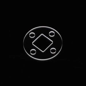
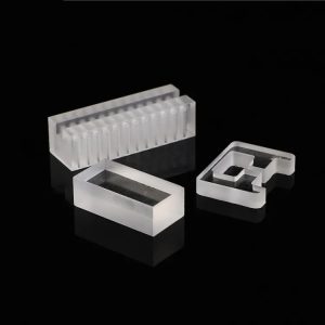
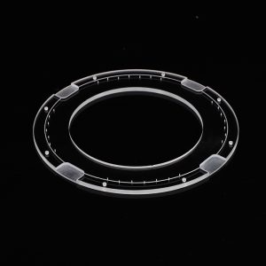
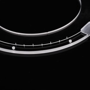
Customizable Shapes & Sizes: Round, square, annular, or sector-shaped wafers with optional polishing, AR/IR/DLC coatings, and microfabrication.
アプリケーション
| Industry | 申し込み | Benefit |
|---|---|---|
| 半導体 | Photomask substrates, etching carriers, CMP polishing pads | High-temperature stability, ultra-low defects, ensures chip manufacturing precision |
| Photovoltaics | PECVD process wafers, thin-film deposition substrates | Thermal shock resistance, improves solar cell efficiency |
| Optoelectronics | LED/LD substrates, laser windows, optical sensors | High UV-IR transmission, low autofluorescence, enhances device performance |
| Precision Optics | Lens substrates, prisms, beam splitters, IR windows | Low thermal expansion, high homogeneity, ensures optical stability |
| Research & Lab | Synchrotron radiation, VUV experiments, high-energy detectors | Radiation-resistant, withstands extreme conditions |
| 航空宇宙 | Satellite optical windows, high-temperature observation panels | Thermal shock endurance, space-grade reliability |
Technical Specifications
| パラメータ | 仕様 |
|---|---|
| 素材 | Synthetic Fused Quartz (SiO₂ ≥99.99%) |
| 直径 | 200 mm (8-inch) |
| Thickness Range | 100 µm – 3000 µm (customizable) |
| Total Thickness Variation (TTV) | ≤10 µm |
| Surface Roughness (Ra) | ≤1.0 nm |
| Total Impurity Content | ≤2.0 µg/g |
| 熱膨張係数 | 0.55 × 10⁻⁶/K (20–300°C) |
| 耐熱温度 | Softening Point 1683°C, short-term up to 1450°C |
| UV Transmittance | >90% (200–260 nm) |
| 表面の平坦度 | High precision, TTV ≤10 µm |
| Shape Options | Round (standard), custom shapes available |
| Certifications | RoHS, ISO9001 |
 よくあるご質問
-
Q: What is the standard thickness of an 8-inch quartz wafer?
A: Standard thickness is 0.5–1.0 mm, with custom options up to 10 mm for specialized semiconductor and optical applications. -
Q: Why choose fused quartz wafers over silicon wafers?
A: Fused quartz wafers provide superior UV transparency, higher thermal stability (up to 1730°C), chemical resistance, and dimensional stability, making them ideal for high-precision lithography and harsh processes. -
Q: Can FUYAO provide custom wafer shapes and surface treatments?
A: Yes. Options include round, square, annular, sector-shaped wafers, with surface treatments such as optical polishing, AR/IR/DLC coatings, drilling, and grooving.


レビュー
レビューはまだありません。