

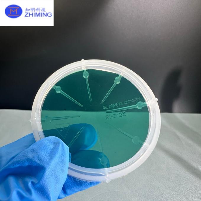


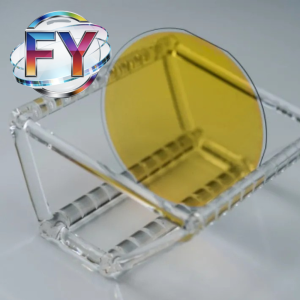
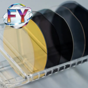
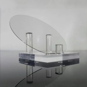
 FUYAO QUARTZ provides high-quality 2-inch 6H-N silicon carbide (SiC) wafers, designed as reliable substrates for advanced semiconductor and power electronic devices. Silicon carbide is a wide-bandgap semiconductor material known for its superior electrical, thermal, and mechanical properties compared with conventional silicon.
The 6H-N SiC polytype offers excellent electrical conductivity, high thermal stability, and strong resistance to harsh environments, making it suitable for power electronics, high-temperature devices, and research applications.
These wafers are manufactured with high crystal quality and low defect density, ensuring stable device fabrication performance and long-term reliability in demanding semiconductor environments.
主な特徴
High Electrical Conductivity
The N-type conductive structure provides stable carrier transport and is suitable for power electronic device fabrication.
Wide Bandgap Semiconductor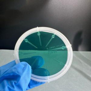
With a bandgap of approximately 3.02 eV, SiC enables operation under high voltage, high temperature, and high-frequency conditions.
High Thermal Conductivity
SiC efficiently dissipates heat generated by high-power devices, improving reliability and device lifetime.
Excellent Mechanical Strength
With a Mohs hardness around 9.2, SiC wafers exhibit strong mechanical durability and wear resistance.
High Breakdown Electric Field
SiC supports high-voltage device structures thanks to its high breakdown field strength.
技術仕様
| パラメータ | 仕様 |
|---|---|
| 素材 | Single Crystal Silicon Carbide |
| Polytype | 6H-N |
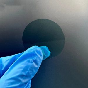
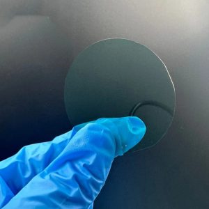
| 直径 | 2 inch (50.8 mm) |
| 厚さ | 350 μm or 650 μm |
| 表面仕上げ | CMP Polished Si-face |
| C-face Treatment | Mechanical Polish |
| 表面粗さ | Ra < 0.2 nm (Si-face) |
| Resistivity | 0.015 – 0.028 Ω·cm |
| Color | Transparent / Light Green |
| パッケージング | Single Wafer Container |
Material Properties of 6H-SiC
| プロパティ | 6H-SiC Value |
|---|---|
| Lattice Parameters | a = 3.073 Å, c = 15.117 Å |
| モース硬度 | ≈ 9.2 |
| 密度 | 3.21 g/cm³ |
| 熱膨張係数 | 4–5 ×10⁻⁶ /K |
| Refractive Index (750 nm) | n₀ = 2.60, nₑ = 2.65 |
| 誘電率 | ≈ 9.66 |
| 熱伝導率 | ~3.7–3.9 W/cm·K |
| Bandgap | 3.02 eV |
| Breakdown Electric Field | 3–5 ×10⁶ V/cm |
| Saturation Drift Velocity | 2.0 ×10⁵ m/s |
アプリケーション
 Power Electronics
Used for high-power and high-voltage semiconductor devices such as diodes, MOSFETs, and power modules.
High-Temperature Electronics
Suitable for devices operating in harsh environments such as aerospace and energy systems.
Research and Semiconductor Development
Widely used as a substrate material for semiconductor research and device prototyping.
Optoelectronic Devices
Applicable in certain optical and photonic applications due to its optical transparency and high refractive index.
よくあるご質問
Q1: What is the difference between 6H-SiC and 4H-SiC wafers?
A: Both 6H-SiC and 4H-SiC are polytypes of silicon carbide with different crystal structures and electrical properties. 4H-SiC typically offers higher electron mobility and is widely used for modern power devices, while 6H-SiC provides stable conductivity and excellent thermal properties, making it suitable for certain power electronics, optoelectronic devices, and research applications.
Q2: What surface finish is provided for the SiC wafer?
A: The silicon face (Si-face) of the wafer is processed with chemical mechanical polishing (CMP) to achieve an ultra-smooth surface with roughness Ra < 0.2 nm, while the carbon face (C-face) is typically mechanically polished. This surface quality ensures compatibility with semiconductor fabrication processes and epitaxial growth requirements.
Q3: Can the wafer specifications be customized?
A: Yes. FUYAO QUARTZ provides customization options including wafer thickness, doping type, resistivity range, surface treatment, and wafer size. Custom specifications can be tailored according to semiconductor device design or research requirements.

レビュー
レビューはまだありません。