
 FUYAO QUARTZ 4-inch A-axis sapphire wafers are high-purity, monocrystalline substrates specifically designed for epitaxial growth and precision LED applications. The A-plane (11-20) orientation provides uniform dielectric properties, excellent insulation, and stable lattice structure, making it ideal for:
-
GaN thin-film epitaxy
-
Hybrid microelectronics
-
Superconducting thin films
Each wafer is manufactured to strict specifications, ensuring ultra-flat surfaces, low roughness, minimal warp/bow, and tight thickness control—critical for high-performance optical and semiconductor applications.
素材特性
-
Ultra-high purity: ≥ 99.999% Al₂O₃ minimizes metallic and ionic contamination.
-
Stable crystallography: Supports epitaxial growth of III-V nitrides, superconductors, and thin films.
-
Surface quality: SSP front surface Ra < 0.5 nm; DSP front & back Ra < 0.5 nm ensures optical-grade smoothness.
-
Mechanical stability: Low warp (<15 μm), low bow (-15 μm to 0 μm), TTV <10 μm.
-
Chemical resistance: Chemically stable and thermally robust for semiconductor and research environments.
Specifications of 4-Inch A-Plane Sapphire Wafers (430 μm)
| パラメータ | 仕様 |
|---|---|
| Crystal Material | ≥ 99.999% High Purity Monocrystalline Al₂O₃ |
| Grade | Prime, Epi-Ready |
| Surface Orientation | A-plane (11-20) |
| 直径 | 100 mm (4 inch), ±0.1 mm |
| 厚さ | 430 μm, ±25 μm |
| Primary Flat Orientation | C-plane (0001), ±0.2° |
| Primary Flat Length | 16.0 mm ±1.0 mm |
| Single Side Polished (SSP) | Front Surface: Epi-polished, Ra <0.5 nm; Back Surface: Fine ground, Ra = 0.8–1.2 μm |
| Double Side Polished (DSP) | Front & Back Surface: Epi-polished, Ra <0.5 nm |
| TTV | < 10 μm |
| お辞儀 | -15 μm to 0 μm |
| ワープ | < 15 μm |
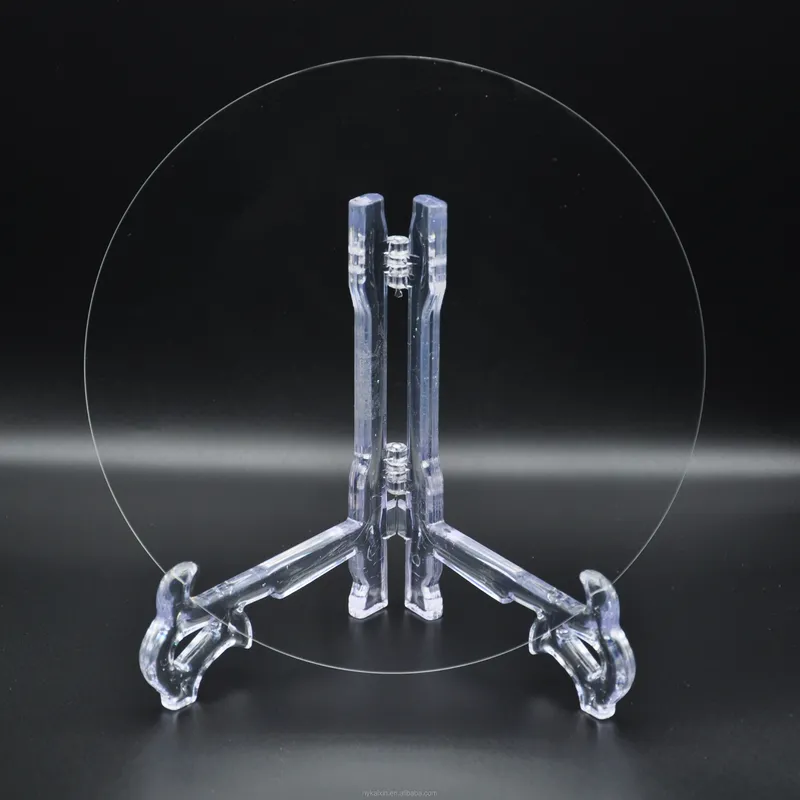
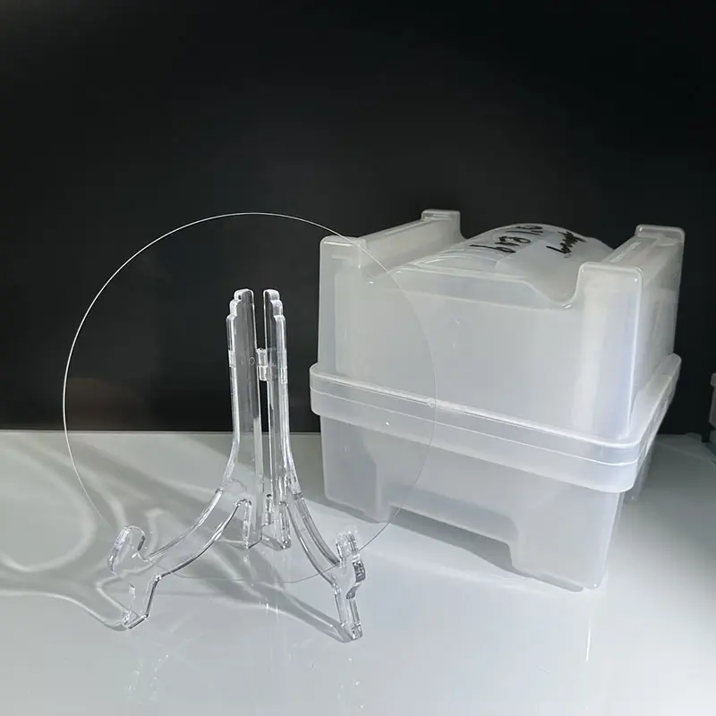
| Cleaning / Packaging | Class 100 cleanroom, vacuum-sealed, 25 pcs per cassette; single-piece packaging available |
| Customization | Any diameter, thickness, orientation, or surface finish can be manufactured |
 アプリケーション
-
LED Epitaxial Growth: Optimal substrate for GaN-based LEDs and III-V nitride thin films.
-
Semiconductor Devices: High insulation and uniform dielectric constant support hybrid microelectronics.
-
Superconductors: Growth of TlBaCaCuO, Tl-2212, and other hetero-epitaxial superconducting thin films.
-
Optics & Thin-Film Applications: Ultra-smooth surfaces allow precise patterning and device fabrication.
-
Research & Development: Ideal for laboratory epitaxy and thin-film experiments.
主な特徴
-
Ultra-high optical and chemical purity
-
優れた熱的・機械的安定性
-
低熱膨張率による正確なアライメント
-
ほとんどの化学試薬に耐性がある
-
Precision-machined surfaces for optimal optical and epitaxial performance
品質保証
FUYAO QUARTZ implements strict quality control, including appearance inspection, dimensional verification, optical performance tests, and parallelism measurement. Each wafer meets international and industry-specific standards, ensuring reliability in high-tech and research environments.
よくあるご質問
-
Can wafers be fully customized?
Yes. FUYAO QUARTZ supports any diameter, thickness, orientation, and SSP/DSP surface finish. -
What is the surface roughness of these wafers?
SSP front surface Ra < 0.5 nm; DSP surfaces Ra < 0.5 nm, suitable for epitaxial growth. -
Which industries use A-plane sapphire wafers?
LED epitaxy, GaN thin films, superconductors, hybrid microelectronics, and optical research. -
What are the tolerances for thickness and flatness?
Thickness ±25 μm, TTV <10 μm, Bow -15 μm to 0 μm, Warp <15 μm.
レビュー
レビューはまだありません。