In semiconductor manufacturing, every step—from silicon wafer growth to photolithography, etching, and chemical vapor deposition (CVD)—places extremely high demands on equipment materials. High-purity fused silica stands out due to its exceptional chemical stability, thermal performance, and broad optical transparency. It plays an irreplaceable role in ensuring process quality, device reliability, and long-term equipment performance. This article explores why high-purity fused silica is critical in semiconductor fabrication and highlights its key functions in equipment design and process optimization.
Core Properties of High-Purity Fused Silica
High-purity fused silica is made from ultra-pure silicon dioxide with extremely low impurity content, often below 1 ppm. Its main characteristics include:
- Minimal metal impurities: Metal ions can introduce crystal defects or reduce photolithography accuracy. The ultra-low impurity content of high-purity fused silica minimizes these risks.
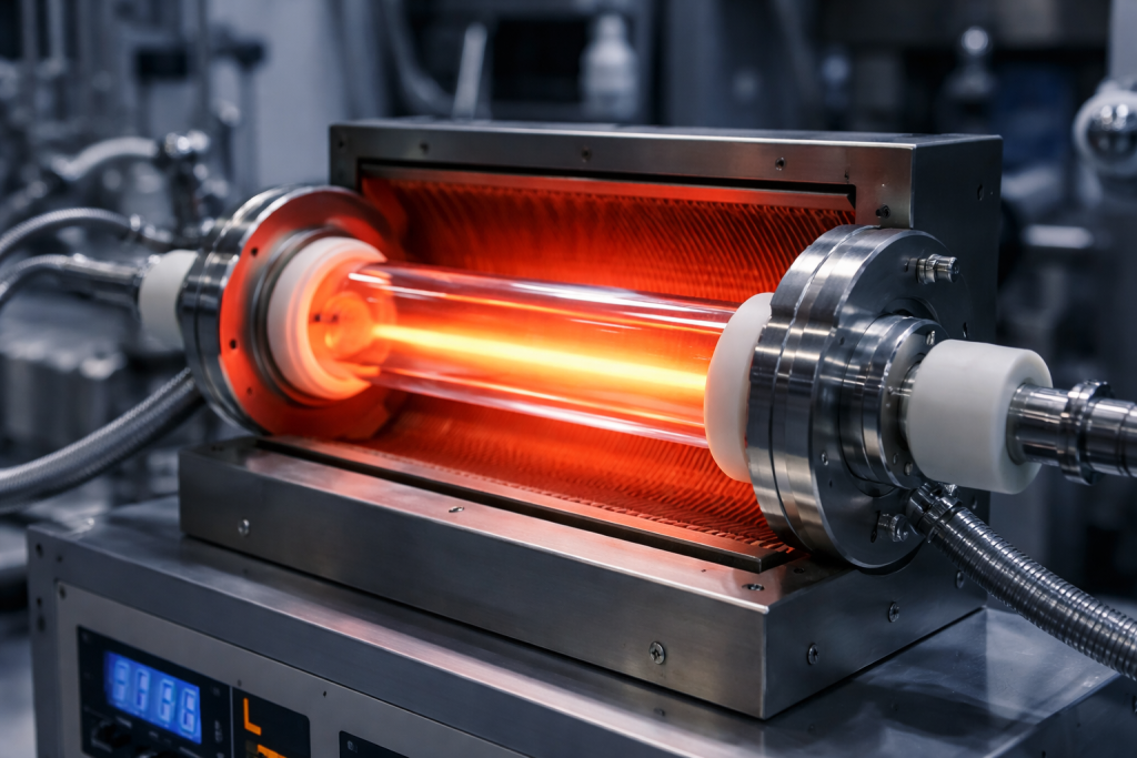
- Excellent thermal stability: With a melting point around 1600°C and a low thermal expansion coefficient, it maintains dimensional stability under high-temperature wafer processing and annealing.
- Outstanding chemical resistance: Resistant to strong acids and bases, it can operate in HF, HCl, or other corrosive gases or solutions without releasing contaminants.
- Wide optical transparency: High transmission from the ultraviolet to near-infrared spectrum makes it suitable for UV photolithography, optical inspection, and in-situ process monitoring.
These properties make high-purity fused silica ideal for meeting the stringent requirements of semiconductor manufacturing equipment, where cleanliness, high-temperature tolerance, and precision are critical.

Typical Applications in Semiconductor Equipment
1. CVD and PECVD Reactor Windows
In chemical vapor deposition (CVD) and plasma-enhanced CVD (PECVD) systems, transparent windows allow operators to monitor deposition processes while maintaining high-temperature, ultra-pure environments. High-purity fused silica windows can withstand high temperatures and aggressive reactive gases without contamination, ensuring stable deposition and high-quality films.
2. Photolithography Exposure Systems
Photolithography requires optical components with high UV transmission and minimal birefringence. High-purity fused silica is ideal for projection lenses, masks, and protective windows due to its exceptional transparency in the deep ultraviolet (DUV) range. Its low thermal expansion ensures that optical alignment remains precise even under prolonged exposure to intense UV light.
3. Etching Chambers and Gas Handling Components
Etching processes, particularly plasma or wet etching, expose equipment to corrosive chemicals. High-purity fused silica components, such as tubes, nozzles, and chamber liners, resist chemical attack and prevent contamination of wafers. This ensures reproducible etching rates and uniform feature definition.
4. Wafer Transport and Handling
Silica-based components are often used in wafer carriers, boat supports, or isolation fixtures because they do not release metallic or ionic impurities. This prevents defect generation during high-temperature processing and reduces particle contamination risks.
Advantages Compared to Other Materials
Compared with standard optical glass or ceramics:
- Glass: While inexpensive and easy to process, ordinary glass has lower thermal and chemical stability and higher impurity content, making it unsuitable for critical semiconductor applications.
- Quartz (crystalline SiO2): Offers good thermal and chemical properties but is more difficult to shape and process in large, complex forms compared to fused silica.
- Ceramics: Certain ceramics are mechanically strong and high-temperature resistant but often lack the optical transparency and low contamination levels needed for UV photolithography or in-situ optical monitoring.
High-purity fused silica provides a unique combination of chemical inertness, thermal resistance, mechanical stability, and optical clarity that is unmatched in semiconductor processing environments.
Design and Process Considerations
When integrating high-purity fused silica components:
- Ensure proper thermal matching with adjacent materials to minimize stress and prevent cracking.
- Maintain a contamination-free environment during handling and installation.
- Consider surface finishing and polishing to reduce scattering and maintain optimal optical performance.
- Evaluate thickness and geometry for pressure or mechanical load, particularly in reactor windows and protective barriers.
These considerations maximize the performance and lifetime of high-purity fused silica components.
Következtetés
High-purity fused silica is a cornerstone material in semiconductor manufacturing. Its combination of ultra-low impurities, exceptional thermal stability, chemical resistance, and wide optical transparency makes it essential for CVD reactors, photolithography systems, etching chambers, and wafer handling equipment. Selecting and integrating high-purity fused silica correctly ensures high device yields, process stability, and long-term reliability in demanding semiconductor environments.