High-purity quartz is one of the most critical materials in modern semiconductor manufacturing. Although often considered a supporting material rather than a core device component, quartz plays a decisive role in ensuring process stability, contamination control, and wafer yield. From crystal growth furnaces to diffusion tubes, plasma etching chambers, and wafer handling systems, semiconductor-grade quartz must meet extremely stringent material and performance standards.
This article provides a technical overview of high-purity quartz used in semiconductor processing, including purity classifications, thermal and mechanical performance requirements, contamination control considerations, and quality evaluation standards.

1. What Is High-Purity Quartz?
High-purity quartz refers to fused silica or synthetic quartz materials with extremely low levels of metallic and alkali impurities. In semiconductor applications, quartz components are typically manufactured from:
- Natural fused quartz (refined from high-grade quartz ore)
- Silice fondue synthétique (produced via chemical vapor deposition or flame hydrolysis)
The primary reason for using quartz is its unique combination of properties:
- High thermal stability
- Low thermal expansion coefficient
- Excellent chemical resistance
- High transparency across UV to IR wavelengths
- Electrical insulation capability
However, in semiconductor manufacturing, these properties alone are not sufficient. Material purity and structural consistency are equally critical.
2. Purity Standards for Semiconductor-Grade Quartz
In advanced semiconductor fabrication, impurity levels are measured in parts per million (ppm) or even parts per billion (ppb). Metallic contaminants such as sodium (Na), potassium (K), lithium (Li), aluminum (Al), iron (Fe), and titanium (Ti) must be tightly controlled.
Typical requirements include:
- Total metallic impurities: often below 10–20 ppm
- Alkali metal content: minimized to prevent ion migration
- Hydroxyl (OH) content: controlled depending on thermal application
Even trace contamination can:
- Alter dopant profiles
- Introduce mobile ion contamination
- Reduce wafer yield
- Cause device leakage or reliability issues
For this reason, semiconductor-grade quartz materials undergo rigorous chemical analysis using techniques such as ICP-MS (Inductively Coupled Plasma Mass Spectrometry) and GDMS (Glow Discharge Mass Spectrometry).
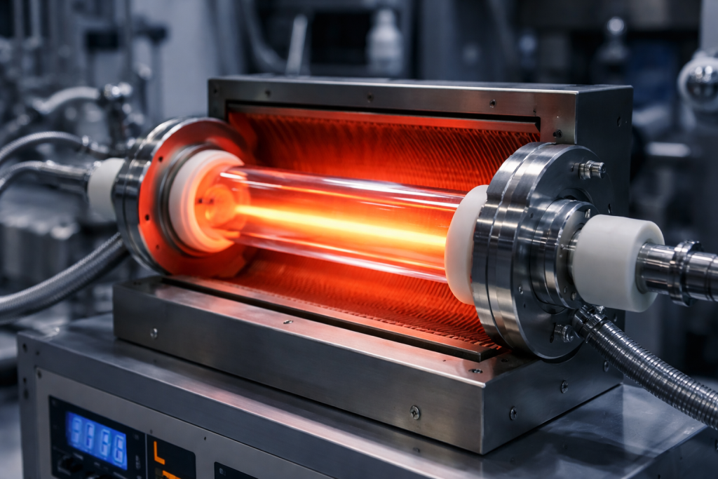
3. Thermal Performance Requirements
Quartz components are widely used in high-temperature processes such as:
- Silicon crystal growth
- Diffusion and oxidation
- Annealing
- Chemical vapor deposition (CVD)
The thermal expansion coefficient of fused quartz is extremely low (approximately 0.5 × 10⁻⁶ /°C), which helps minimize thermal stress and deformation. However, quartz must also demonstrate:
- Strong resistance to thermal shock
- Minimal devitrification at elevated temperatures
- Long-term dimensional stability
In crystal growth furnaces, quartz tubes and crucibles are exposed to sustained temperatures above 1000°C. Any deformation, softening, or impurity diffusion at these temperatures can negatively impact process uniformity and crystal quality.
4. Mechanical and Structural Requirements
Although quartz is chemically stable, it is inherently brittle. Therefore, mechanical design considerations are critical.
Key structural requirements include:
- Uniform wall thickness
- Low internal stress
- Absence of microcracks or bubbles
- High surface finish quality
Microdefects can propagate under repeated thermal cycling, leading to fracture or particle generation. In semiconductor equipment, particle contamination is one of the primary yield risks. Therefore, quartz components must undergo annealing treatments to relieve internal stress and improve structural integrity.
5. Chemical Resistance in Plasma and Reactive Environments
Quartz components are frequently exposed to aggressive chemical environments, including:
- Plasma etching gases
- Reactive fluorine-based chemistries
- Oxidizing atmospheres
Fused quartz exhibits excellent resistance to most acids except hydrofluoric acid (HF). However, prolonged plasma exposure may cause:
- Surface roughening
- Micro-erosion
- Structural weakening
To mitigate degradation, manufacturers may optimize material density and surface finishing processes. In some cases, alternative materials such as high-density alumina are considered for extreme plasma conditions, but quartz remains preferred due to its purity and process compatibility.
6. Optical and Electrical Considerations
Quartz is highly transparent across ultraviolet (UV), visible, and infrared (IR) spectra. This property makes it suitable for:
- Optical monitoring windows
- UV curing systems
- Lithography support structures
In addition, quartz provides excellent electrical insulation, making it ideal for high-voltage or RF environments.
However, optical-grade quartz used in semiconductor tools must meet additional criteria:
- Minimal birefringence
- Low bubble density
- Uniform refractive index
These factors ensure consistent optical performance in high-precision processing systems.
7. Quality Control and Inspection Standards
To ensure reliability in semiconductor environments, quartz components undergo comprehensive quality inspection:
- Visual inspection for inclusions and bubbles
- Surface roughness measurement
- Dimensional tolerance verification
- Chemical impurity testing
- Thermal stress evaluation
For large-diameter wafer production platforms, dimensional stability becomes increasingly critical. Even slight geometric deviations can affect wafer positioning or thermal uniformity inside processing chambers.
8. Role in Wide Bandgap Semiconductor Manufacturing
As wide bandgap semiconductors such as silicon carbide (SiC) gain importance, process temperatures and power densities increase. This places additional demands on quartz materials:
- Higher thermal endurance
- Greater structural stability
- Improved contamination resistance
In crystal growth systems for advanced materials, quartz components must withstand extreme conditions without compromising purity or mechanical integrity.
9. Challenges and Industry Trends
Despite its advantages, high-purity quartz faces several challenges:
- Increasing demand for larger wafer sizes
- Stricter contamination standards
- Supply chain constraints for ultra-high-purity raw materials
- Cost pressures in advanced manufacturing
To address these challenges, manufacturers are investing in:
- Improved refining technologies
- Better stress-relief annealing methods
- Enhanced impurity detection techniques
- Automation in precision machining
These developments aim to maintain high reliability while supporting next-generation semiconductor fabrication.
Conclusion
High-purity quartz is not merely a structural material in semiconductor equipment—it is a critical enabler of process stability and device reliability. Its chemical purity, thermal stability, mechanical integrity, and optical performance must all meet rigorous industry standards.
As semiconductor manufacturing advances toward higher temperatures, tighter tolerances, and larger wafer platforms, the role of high-purity quartz becomes even more significant. Selecting the appropriate quartz material requires careful consideration of purity levels, thermal requirements, structural quality, and application-specific conditions.
In high-performance semiconductor processing, material selection is never trivial. High-purity quartz remains a foundational material precisely because it delivers consistent, reliable performance under some of the most demanding manufacturing environments in the world.