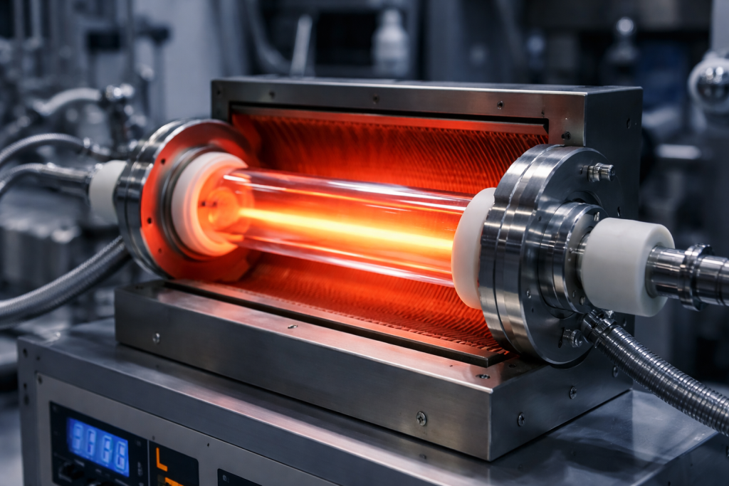
As semiconductor device dimensions continue to shrink and process nodes become increasingly advanced, contamination control has become one of the most critical factors in wafer manufacturing. While engineers often focus on process gases, cleanroom standards, and equipment precision, one overlooked source of contamination is the quartz components used inside equipos semiconductores.
Quartz parts are widely used in diffusion furnaces, oxidation systems, etching equipment, and CVD processes because of their high purity, excellent thermal stability, and resistance to harsh chemicals. However, not all quartz materials are equal. Even trace levels of metallic impurities can significantly affect wafer yield and device performance.
For semiconductor applications, ultra-low metal contamination is not optional—it is a fundamental requirement.
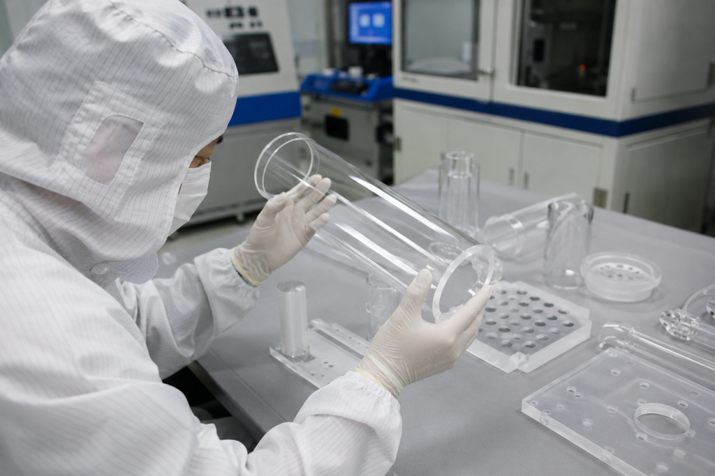
Why Quartz Is Widely Used in Semiconductor Manufacturing
High-purity fused quartz has become a standard material in semiconductor environments due to its unique combination of properties:
- Excellent thermal resistance above 1000°C
- Extremely low coefficient of thermal expansion
- High purity silicon dioxide structure
- Strong resistance to corrosive chemicals
- Baja generación de partículas
- Stability under repeated thermal cycling
Typical semiconductor quartz components include:
- Tubos de cuarzo para hornos
- Portaoblas
- Embarcaciones de cuarzo
- Shower heads
- Quartz rings
- Cámaras de proceso
- Ventanas de cuarzo
- Customized quartz plates and fixtures
These components operate in direct proximity to silicon wafers during critical process steps. Any contamination released from the material can be transferred directly onto the wafer surface.
Why Trace Metals Matter in Semiconductor Processing
In conventional industrial applications, metal impurities at several ppm may be acceptable. Semiconductor manufacturing is very different.
Even extremely low concentrations of metallic contaminants can create process instability and device defects.
Common harmful metal impurities include:
| Metal Element | Potential Impact |
|---|---|
| Aluminio (Al) | Alters electrical characteristics |
| Hierro (Fe) | Creates carrier recombination centers |
| Sodio (Na) | Causes mobile ion contamination |
| Potasio (K) | Degrades dielectric reliability |
| Calcio (Ca) | Generates unwanted particles |
| Litio (Li) | Affects gate oxide integrity |
For advanced semiconductor production, impurity levels often need to remain below:
- Al <1 ppm
- Fe <1 ppm
- Na <1 ppm
- K <1 ppm
Some critical applications require concentrations measured in parts per billion (ppb).
Although these values appear extremely small, modern semiconductor devices operate at scales where atomic-level contamination can impact performance.
How Metal Contamination Reaches the Wafer
Metal impurities can enter semiconductor processes through several pathways.
Material-Origin Contamination
Raw quartz materials may naturally contain residual metallic elements. Lower-grade quartz sources often contain aluminum, alkali metals, and transition metals.
Without purification, these contaminants remain trapped inside the quartz structure.
High-Temperature Diffusion
Semiconductor furnaces frequently operate between 900°C and 1200°C.
At elevated temperatures, metallic impurities can migrate from quartz surfaces and diffuse into process environments.
This issue becomes particularly severe during:
- Thermal oxidation
- Procesos de difusión
- LPCVD deposition
- Annealing operations
Surface Particle Generation
Poor processing methods may create:
- Micro-cracks
- Surface defects
- Residual machining contamination
These defects become particle sources during thermal cycling.
Particle contamination can lead to:
- Pattern defects
- Wafer scratching
- Yield reduction
Effects on Wafer Yield
Ultra-fine semiconductor structures have very low tolerance for contamination.
Potential consequences include:
Increased Defect Density
Metal atoms can become embedded in active device regions and create electrical defects.
Reduced Device Reliability
Impurities may alter dielectric behavior and reduce long-term device stability.
Lower Process Repeatability
Contamination introduces process variation, making production less predictable.
Yield Loss
Even a minor increase in contamination may translate into significant financial losses in high-volume manufacturing.
For fabs processing thousands of wafers per month, a small yield reduction can represent substantial production costs.
How High-Purity Semiconductor Quartz Is Manufactured
Producing semiconductor-grade quartz requires much more than standard quartz melting.
Several critical steps are involved:
Selection of High-Purity Raw Material
Only carefully refined silica sources with extremely low impurity levels are selected.
Advanced Purification Processes
Chemical purification removes trace metallic contaminants before melting.
Typical methods include:
- Limpieza con ácido
- High-temperature refining
- Controlled purification procedures
Clean Manufacturing Environment
Quartz fabrication for semiconductor use often takes place in controlled clean environments to minimize particle introduction.
Precision Surface Processing
Advanced polishing and cleaning processes reduce:
- Surface roughness
- Residual particles
- Micro-cracks
These steps improve contamination resistance and service life.
Typical Semiconductor Quartz Purity Requirements
| Propiedad | Semiconductor Grade Quartz |
|---|---|
| SiO₂ Purity | >99.99% |
| Aluminio (Al) | <1 ppm |
| Hierro (Fe) | <1 ppm |
| Sodio (Na) | <1 ppm |
| Potasio (K) | <1 ppm |
| Calidad de la superficie | Baja generación de partículas |
| Estabilidad térmica | Excelente |
Actual specifications vary depending on process requirements and equipment design.
Selecting a Quartz Supplier for Semiconductor Applications
When evaluating a quartz supplier, price alone should never be the deciding factor.
Consider the following:
- Raw material traceability
- Metal impurity analysis capability
- Surface cleanliness standards
- Precision machining capability
- Thermal process experience
- Custom design support
- Semiconductor industry experience
Reliable suppliers should provide material analysis reports and maintain strict contamination control throughout manufacturing.
Reflexiones finales
As semiconductor technology advances, contamination tolerance continues to shrink. Quartz components are no longer simply structural parts inside process equipment—they are critical contributors to yield stability and process reliability.
Ultra-low metal contamination directly affects wafer quality, equipment performance, and manufacturing cost. Choosing semiconductor-grade high-purity quartz is an investment in long-term process control rather than a simple material decision.
For high-temperature semiconductor environments, purity is not just a specification on paper—it is a requirement that determines production success.
PREGUNTAS FRECUENTES
What purity level is required for semiconductor quartz parts?
Most semiconductor applications require quartz purity above 99.99%, with metal contaminants such as Al, Fe, Na, and K typically controlled below 1 ppm.
Why are sodium and potassium considered harmful contaminants?
These alkali metals can migrate under electric fields and create instability in semiconductor devices, especially in gate oxide structures.
Can standard industrial quartz be used in semiconductor furnaces?
Generally no. Industrial-grade quartz may contain higher metal impurities and particles, which can negatively impact wafer yield and process reliability.