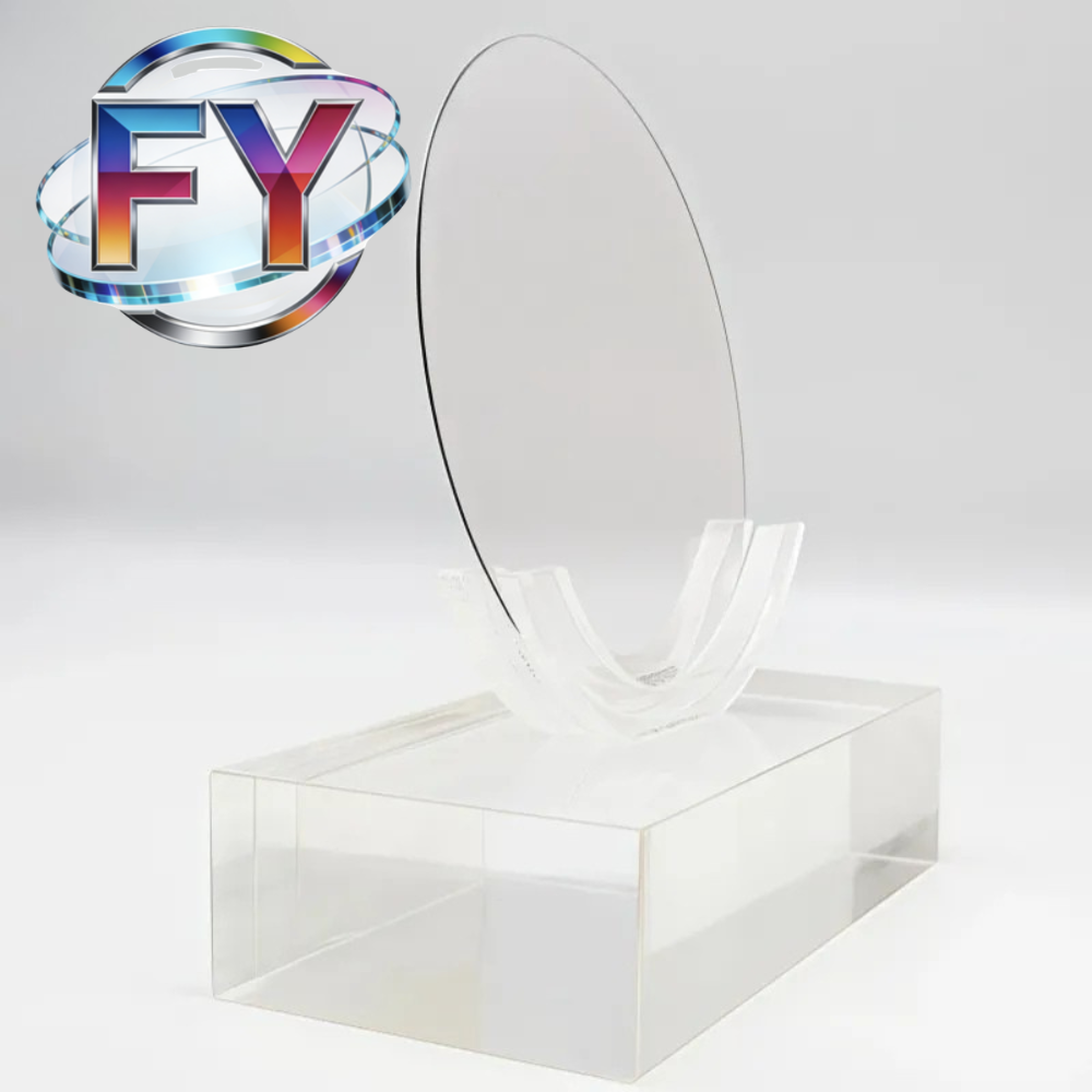
BF33 glass wafers are widely used in MEMS packaging, wafer bonding, optical sensors, microfluidic devices, precision windows, and semiconductor-related glass components. For many engineering projects, selecting the right BF33 glass wafer thickness is just as important as choosing the material itself. A wafer that is too thin may crack during handling or bonding, while a wafer that is too thick may increase package height, optical path length, machining cost, and thermal stress risk.
BF33 glass, often known as BOROFLOAT33 borosilicate glass, is valued for its low thermal expansion, good flatness, optical transparency, chemical durability, and process stability. Standard BOROFLOAT33 sheets are available in a broad thickness range, with supplier technical data listing common thickness availability from 0.7 mm up to 25.4 mm depending on sheet format.
For engineers designing MEMS devices, optical packages, or custom glass wafer components, thickness selection should be based on the final application, bonding method, mechanical strength, flatness requirement, optical performance, and processing route.
1. Start with the Application
The first question is simple: what function does the BF33 glass wafer need to perform?
In MEMS packaging, BF33 glass may be used as a cap wafer, support wafer, bonding wafer, pressure sensor cover, or transparent protective lid. In optical packaging, it may serve as a window, cover glass, sensor protection plate, or optical interface. In microfluidic applications, it may be used as a channel cover, bonding substrate, or transparent inspection layer.
Each application has different thickness priorities:
| Anmeldung | Thickness Selection Focus |
|---|---|
| MEMS cap wafer | Bonding flatness, cavity depth, stress control |
| Optical window | Transmission, rigidity, optical path length |
| Microfluidic chip | Bonding strength, channel protection, transparency |
| Sensor package | Mechanical protection, sealing, package height |
| Temporary carrier | Strength, flatness, thermal stability |
| Custom glass part | Machining allowance, hole drilling, edge strength |
For a small MEMS sensor package, a thinner BF33 wafer may help reduce device height. For a large optical window or carrier wafer, a thicker wafer may be necessary to improve rigidity and reduce breakage risk.
2. Consider Mechanical Strength and Handling Risk
Thin glass wafers are attractive because they reduce weight and package thickness, but they are more fragile during cutting, cleaning, bonding, dicing, inspection, and transportation. As wafer diameter increases, handling risk also increases.
For small-diameter wafers or small diced glass parts, thinner BF33 may be practical. For larger wafers or parts with holes, slots, steps, or complex edges, more thickness may be needed to maintain strength during processing.
Engineers should consider:
- Wafer diameter or part size
- Whether the wafer will be diced after bonding
- Whether holes, grooves, or cavities are required
- Cleaning and packaging method
- Assembly pressure or clamping force
- Risk of edge chipping during handling
- Final product shock or vibration environment
A very thin wafer may pass material inspection but fail during downstream processing. Therefore, the final process flow should be considered before confirming thickness.
3. Match Thickness with Wafer Bonding Requirements
BF33 glass is commonly used in glass-to-silicon bonding, including anodic bonding for MEMS devices. Silicon-glass bonding is widely used in MEMS and NEMS packaging, and anodic bonding is often selected because it can provide strong bonding without an additional adhesive layer.
For bonding applications, thickness affects several important factors:
- Thermal stress after bonding
- Wafer bow and deformation
- Bonding pressure distribution
- Cavity sealing performance
- Device package height
- Dicing stability after bonding
In silicon-to-glass structures, thermal expansion mismatch can generate residual stress during cooling after bonding. Research on silicon-glass anodic bonding has shown that residual stress is affected by thermal expansion behavior and the thickness ratio between silicon and glass layers.
This means BF33 wafer thickness should not be selected only by availability. It should be matched with the silicon wafer thickness, bonding temperature, device structure, and stress tolerance of the MEMS design.
4. Balance Rigidity and Package Height
In many optical and MEMS packages, engineers want the glass wafer to be thin enough for compact design but thick enough to remain rigid.
A thicker BF33 wafer generally provides better mechanical rigidity and lower risk of bending during handling. However, it also increases package height and material cost. In optical applications, thickness may also increase optical path length and may affect focus, transmission, and system calibration.
For compact sensor packages, thinner BF33 glass can reduce final device thickness. For larger optical windows or carrier wafers, thicker BF33 glass may be more stable. The right choice is often a compromise between mechanical safety and design compactness.
5. Check TTV, Bow, Warp, and Flatness
Thickness is not only a nominal number. For precision wafers, engineers also need to check thickness uniformity and shape control.
Important parameters include:
| Parameter | Meaning | Why It Matters |
| Dicke | Nominal wafer thickness | Affects strength, package height, optical path |
| TTV | Total thickness variation | Affects bonding uniformity and lithography compatibility |
| Bogen | Curvature of the wafer center relative to edges | Affects bonding and alignment |
| Warp | Overall wafer deformation | Affects process stability |
| Surface roughness | Surface smoothness after polishing | Important for bonding, coating, and optics |
| Kantenqualität | Chamfer, bevel, or rounded edge condition | Reduces cracking and chipping |
For MEMS bonding and optical packaging, a wafer with suitable thickness but poor TTV or excessive bow may still cause bonding defects or assembly failure.
6. Consider Optical Performance
For optical packaging, BF33 wafer thickness can influence optical performance. A thicker glass window may provide better strength, but it may also increase absorption, reflection, and optical path deviation. This is especially important for imaging systems, optical sensors, laser modules, and inspection windows.
BF33 glass is known for good optical clarity and broad transparency, which makes it suitable for many visible and near-infrared optical applications. However, engineers should still consider:
- Operating wavelength range
- Transmission requirement
- Reflection loss
- Need for anti-reflective coating
- Surface quality requirement
- Parallelism and wedge angle
- Optical distortion tolerance
If the component is used only as a protective cover, thickness may mainly depend on strength. If it is part of an optical path, thickness, flatness, parallelism, and coating design become more important.
7. Think About Machining and Custom Processing
Many BF33 wafers are not used as simple round wafers. They may require custom cutting, drilling, slotting, polishing, edge grinding, coating, or cleaning. Thickness affects the difficulty and yield of these processes.
For example, very thin BF33 wafers may be difficult to drill without breakage. Very thick wafers may require longer processing time and may increase cost. If the design includes holes, steps, inner corners, or narrow bridges, engineers should leave enough thickness to support machining stability.
Common custom processing options include:
- Round wafer cutting
- Square or rectangular glass substrate cutting
- Hole drilling
- Slot machining
- Edge beveling
- Surface polishing
- Beidseitiges Polieren
- AR or protective coating
- Semiconductor-grade cleaning
- Custom wafer packaging
Before ordering, it is better to provide drawings with thickness, tolerance, surface quality, and edge requirements clearly marked.
8. Select Thickness by Practical Design Range
Although every project is different, the following general guidance can help engineers make an initial selection:
| BF33 Thickness Range | Typische Verwendung |
| 0.3–0.7 mm | Thin covers, lightweight packages, compact MEMS parts |
| 0.7–1.1 mm | Common MEMS cap wafers, small optical covers, sensor windows |
| 1.1–2.0 mm | General optical windows, bonding substrates, stronger glass caps |
| 2.0–5.0 mm | Rigid windows, carrier plates, machined glass components |
| Above 5.0 mm | Thick optical parts, structural glass components, special custom parts |
This table is only a design reference. Final thickness should be confirmed based on wafer diameter, tolerance, bonding process, strength requirement, and downstream processing.
9. Do Not Ignore Tolerance
Thickness tolerance can be as important as thickness itself. Standard BOROFLOAT® 33 sheet tolerance varies by thickness range, and processing suppliers may also provide tighter custom wafer tolerances through grinding and polishing. For example, published technical information shows different tolerance ranges for different sheet thicknesses, with thinner sheets generally having tighter standard thickness tolerance than thicker sheets.
For precision wafers, engineers should define whether they need standard sheet tolerance, ground tolerance, polished wafer tolerance, or semiconductor-grade TTV control. A vague request such as “1 mm BF33 wafer” may not be enough for MEMS or optical packaging.
A better inquiry should include:
- Diameter or length × width
- Thickness and tolerance
- TTV requirement
- Bow and warp requirement
- Surface roughness
- SSP or DSP
- Edge type
- Hole or slot details
- Coating requirement
- Cleaning and packaging requirement
- Quantity and application
10. Cost and Lead Time Considerations
Thickness also affects cost and lead time. Common thicknesses are usually easier to source and process. Unusual thickness, tight TTV, high flatness, double-side polishing, precision holes, and special coatings may increase cost and production time.
For early-stage R&D, engineers may choose a standard thickness first to verify the design. For mass production, the thickness should be optimized based on yield, handling safety, process compatibility, and total cost.
Schlussfolgerung
BF33 glass wafer thickness selection should not be based only on a standard catalog size. Engineers need to consider the real function of the wafer, including MEMS bonding, optical transmission, mechanical protection, processing stability, and final package requirements.
A thinner BF33 wafer may reduce weight and package height, but it also increases handling and breakage risk. A thicker wafer may improve rigidity and strength, but it can increase cost, optical path length, and package size. For MEMS and optical packaging, the best thickness is usually the one that balances strength, flatness, bonding reliability, optical performance, and manufacturability.
Before placing an order, buyers should confirm thickness, tolerance, TTV, bow, warp, surface finish, edge quality, coating, cleaning grade, and packaging method. These details can directly affect bonding yield, optical performance, and long-term device reliability.