In der modernen Halbleiterfertigung spielt die Materialwissenschaft eine ebenso wichtige Rolle wie die Anlagen selbst. Unter allen funktionalen Materialien sticht hochreines Quarz (SiO₂) als unverzichtbares Rückgrat in fast jeder Phase der Chip-Herstellung hervor - von der Silizium-Einkristallzüchtung bis zur fortschrittlichen Wafer-Verarbeitung. Dank seiner außergewöhnlichen Reinheit, hohen thermischen Beständigkeit, chemischen Inertheit und optischen Transparenz sind Quarzkomponenten für die Aufrechterhaltung der extrem sauberen und streng kontrollierten Umgebungen, die in Halbleiterfabriken erforderlich sind, unerlässlich.
1. Grundlegende Eigenschaften von Quarz und Prozesskompatibilität
Der weit verbreitete Einsatz von Quarz in Halbleiteranlagen ist auf seine einzigartigen physikalischen und chemischen Eigenschaften zurückzuführen:
- Höchste Reinheit (4N8 und höher): Metallische Verunreinigungen können bis auf ppm- oder sogar ppb-Niveau kontrolliert werden
- Ausgezeichnete thermische Stabilität: Schmelzpunkt über 1700°C, bei Langzeitbetrieb über 1100-1200°C
- Niedriger Wärmeausdehnungskoeffizient: Minimiert die thermische Belastung und Verformung
- Hervorragende chemische Beständigkeit: Stabil gegen die meisten Säuren und Gase außer Flusssäure (HF)
- Hohe optische Transparenzგანსაკუთრებით wirksam bei ultravioletten (UV) Wellenlängen
Dank dieser Eigenschaften kann Quarz nicht nur als Konstruktionsmaterial, sondern auch als integraler Bestandteil der Prozessumgebung selbst fungieren.
2. Silizium-Kristallwachstum: Die fundamentale Rolle von Quarz-Tiegeln
Beim Czochralski-Verfahren (CZ) sind Quarztiegel unverzichtbare Verbrauchsmaterialien, die zum Schmelzen von Polysilizium und zum Züchten von einkristallinen Siliziumblöcken verwendet werden.
Wichtige technische Anforderungen:
| Parameter | Typische Spezifikation |
|---|---|
| Reinheit | ≥ 99,998% (4N8) |
| Betriebstemperatur | 1400-1600°C |
| Sauerstoffkontrolle | Entscheidend für das Defect Engineering |
| Dimensionsstabilität | Verhindert Verformungen während des Wachstums |
Quarzschmelztiegel beeinflussen den Sauerstoffeintrag in die Siliziumschmelze, was sich unmittelbar auf Kristalldefekte und elektrische Eigenschaften auswirkt. Daher werden sowohl die Qualität des Rohmaterials als auch die Herstellungsverfahren (z. B. Lichtbogenschmelzen, Rotationsformen) streng kontrolliert.
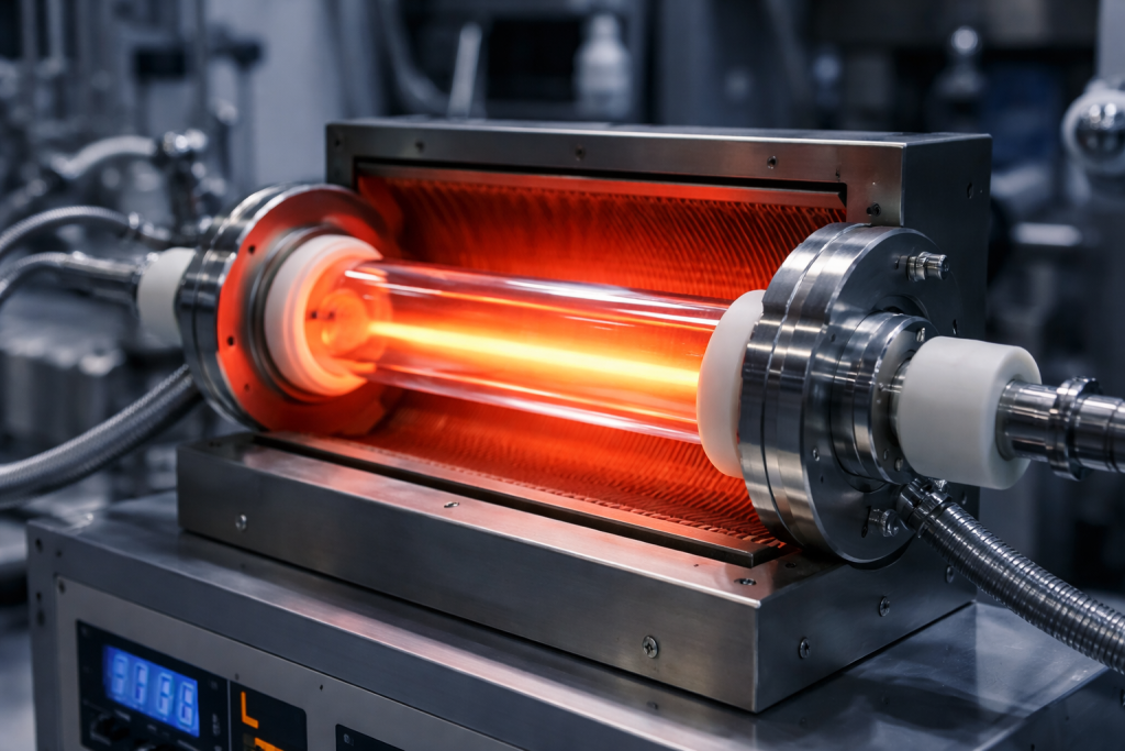
3. Verarbeitung bei hohen Temperaturen: Quarzrohre und Boote
Quarzkomponenten werden in großem Umfang verwendet in Diffusion, Oxidation und chemische Gasphasenabscheidung (CVD) Prozesse.
3.1 Quarzröhren
Quarzröhren dienen als Hochtemperatur-Reaktionskammern:
- Dauerbetrieb über 1100°C
- Äußerst geringe Metallkontamination (≤1 ppm)
- Hohe Beständigkeit gegen Temperaturschock und Verformung
3.2 Quarzboote
Quarzboote werden verwendet, um mehrere Wafer während der Stapelverarbeitung zu tragen:
- Kompatibel mit 4-Zoll- bis 12-Zoll-Wafern
- Erhältlich in vertikalen und horizontalen Konfigurationen
- Sie erfordern eine hohe mechanische Festigkeit und eine äußerst geringe Partikelbildung
Zusammen bilden diese Komponenten das Rückgrat der thermischen Verarbeitungssysteme in Waferfabriken und wirken sich direkt auf die Ausbeute und die Prozessgleichmäßigkeit aus.
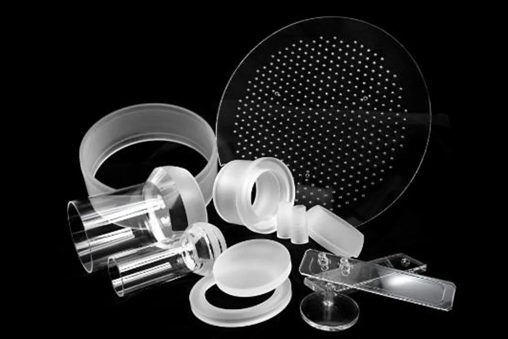
4. Ätzen und Abscheidung: Quarz-Strukturkomponenten
Bei Plasmaätz- und Dünnschichtabscheidungsverfahren (wie PVD, CVD und ALD), fungieren Quarzteile als kritische Struktur- und Schutzelemente.
Typische Quarzkomponenten:
- Quarzringe und Fokusringe: Aufrechterhaltung der Plasmagleichmäßigkeit und Schutz der Kammerwände
- Flansche aus Quarz: Sicherstellung der Vakuumversiegelung und der Systemintegrität
- Quarz-Injektoren: Präzise Förderung von Prozessgasen oder -flüssigkeiten
Diese Komponenten müssen Plasmabestrahlung, reaktiven Gasen und hochenergetischem Ionenbeschuss standhalten und gleichzeitig Maßhaltigkeit und Sauberkeit gewährleisten.
5. Reinigungsprozesse: Quarz-Tanks und -Träger
Die Nassreinigung ist ein wichtiger Schritt bei der Halbleiterherstellung, bei dem Chemikalien wie HF, H₂SO₄ und NH₄OH zum Einsatz kommen.
Quarzanwendungen in der Reinigung:
- Quarz-Reinigungsbehälter: مقاومة starke Säuren und hohe Temperaturen
- Quarz-Körbe (Träger): Halten der Wafer während der chemischen Reinigung
- Quarz-Flüssigkeitssammelflaschen: Sammeln und Lagern von Chemikalienresten ohne Kontamination
Quarz sorgt dafür, dass bei der Reinigung keine zusätzlichen Verunreinigungen eingebracht werden, was für fortschrittliche Knotenpunkte, bei denen die Kontaminationskontrolle extrem streng ist, von entscheidender Bedeutung ist.
6. Fortgeschrittene Anwendungen: Quarzgläser und Fotolithografie
6.1 Quarzglockengläser
Quarzglocken sind weit verbreitet in:
- Reaktoren zur Herstellung von Polysilizium
- Systeme für epitaktisches Wachstum
Sie sorgen für eine kontrollierte Reaktionsumgebung und ermöglichen eine gleichmäßige Wärmestrahlungsübertragung, was für die Prozessstabilität und die Gleichmäßigkeit des Films unerlässlich ist.
6.2 Fotolithografie und optische Komponenten
Quarz wird aufgrund seiner hohen UV-Transparenz auch in optischen Anwendungen eingesetzt:
- Quarz-Fotomasken: Dienen als “Master-Vorlagen” für die Übertragung von Mustern
- Quarz-Fenster: Ermöglicht präzise UV-Belichtung in Lithografiesystemen
Diese Komponenten sind für eine hochauflösende Strukturierung in modernen Halbleiterknoten unerlässlich.
7. Prozessüberwachung: Quarzkristall-Sensoren
Bei der Dünnschichtabscheidung werden Quarzkristall-Mikrowaagen-Sensoren (QCM) eingesetzt, um die Schichtdicke in Echtzeit zu überwachen. Diese Sensoren beruhen auf der Frequenzänderung eines vibrierenden Quarzkristalls, um die Massenabscheidung mit hoher Präzision zu messen und so Gleichmäßigkeit und Prozesskontrolle zu gewährleisten.
8. 2026 Trends: Höhere Reinheit, größere Größen und Lokalisierung
Mit der fortschreitenden Entwicklung der Halbleitertechnologie werden an Quarzkomponenten immer höhere Anforderungen gestellt:
8.1 Höhere Reinheitsstandards
Moderne Knotenpunkte verlangen Verunreinigungswerte unter ppb, was die Entwicklung von synthetischem Quarz gegenüber natürlichem Quarz vorantreibt.
8.2 Größere Abmessungen
Mit dem Übergang zu größeren Wafern (300 mm und mehr) müssen Quarzkomponenten entsprechend skaliert werden, wobei die strukturelle Integrität erhalten bleiben muss.
8.3 Verbesserte Langlebigkeit
Längere Lebenszyklen von Anlagen und härtere Prozessbedingungen erfordern eine verbesserte Beständigkeit gegen Plasmaerosion und Temperaturwechsel.
8.4 Lokalisierung und Sicherheit der Lieferkette
Aufgrund der Dynamik der globalen Lieferkette wird die inländische Fertigung von hochwertigen Quarzkomponenten zu einer strategischen Priorität, insbesondere in den aufstrebenden Halbleitermärkten.
Schlussfolgerung
Quarz-Komponenten sind weit mehr als nur Hilfsmaterialien in der Halbleiterfertigung - sie sind die Grundlage für Prozessstabilität, Reinheit und Präzision. Vom Kristallwachstum und der thermischen Verarbeitung bis hin zum Ätzen, Reinigen und der Fotolithografie spielt Quarz in jeder Phase eine entscheidende Rolle.
Mit dem Vorstoß der Halbleiterindustrie in anspruchsvollere technologische Knotenpunkte im Jahr 2026 und darüber hinaus werden die Anforderungen an Quarzmaterialien - Reinheit, Leistung und Präzision - weiter steigen. Dies stellt nicht nur technische Herausforderungen dar, sondern schafft auch Möglichkeiten für Innovation und Lokalisierung in der globalen Halbleiterlieferkette.